
© 2000 Fairchild Semiconductor Corporation
DS006386
www.fairchildsemi.com
August 1986
Revised April 2000
DM74LS123
Dual
Ret
ri
ggerabl
e
O
n
e
-Shot
wit
h
C
lear
and
Com
p
lementa
ry
O
u
tput
s
DM74LS123
Dual Retriggerable One-Shot
with Clear and Complementary Outputs
General Description
The DM74LS123 is a dual retriggerable monostable multi-
vibrator capable of generating output pulses from a few
nano-seconds to extremely long duration up to 100% duty
cycle. Each device has three inputs permitting the choice of
either leading edge or trailing edge triggering. Pin (A) is an
active-LOW transition trigger input and pin (B) is an active-
HIGH transition trigger input. The clear (CLR) input termi-
nates the output pulse at a predetermined time indepen-
dent of the timing components. The clear input also serves
as a trigger input when it is pulsed with a low level pulse
transition (
). To obtain the best trouble free operation
from this device please read the operating rules as well as
the Fairchild Semiconductor one-shot application notes
carefully and observe recommendations.
Features
■
DC triggered from active-HIGH transition or active-LOW
transition inputs
■
Retriggerable to 100% duty cycle
■
Compensated for V
CC
and temperature variations
■
Triggerable from CLEAR input
■
DTL, TTL compatible
■
Input clamp diodes
Ordering Code:
Devices also available in Tape and Reel. Specify by appending the suffix letter “X” to the ordering code.
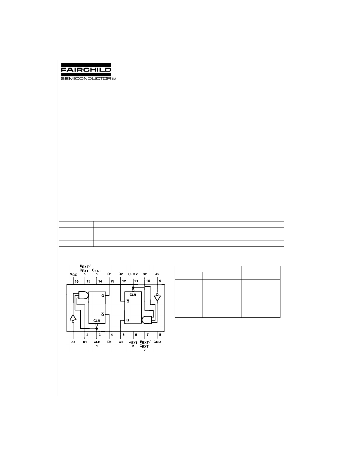
Connection Diagram
Function Table
H
=
HIGH Logic Level
L
=
LOW Logic Level
X
=
Can Be Either LOW or HIGH
↑
=
Positive Going Transition
↓
=
Negative Going Transition
=
A Positive Pulse
=
A Negative Pulse
Order Number
Package Number
Package Description
DM74LS123M
M16A
16-Lead Small Outline Integrated Circuit (SOIC), JEDEC MS-012, 0.150 Narrow
DM74LS123SJ
M16D
16-Lead Small Outline Package (SOP), EIAJ TYPE II, 5.3mm Wide
DM74LS123N
N16E
16-Lead Plastic Dual-In-Line Package (PDIP), JEDEC MS-001, 0.300 Wide
Inputs
Outputs
CLEAR
A
B
Q
Q
L
X
X
L
H
X
H
X
L
H
X
X
L
L
H
H
L
↑
H
↓
H
↑
L
H
www.fairchildsemi.com
2
DM74LS123
Functional Description
The basic output pulse width is determined by selection of
an external resistor (R
X
) and capacitor (C
X
). Once trig-
gered, the basic pulse width may be extended by retrigger-
ing the gated active-LOW transition or active-HIGH
transition inputs or be reduced by use of the active-LOW or
CLEAR input. Retriggering to 100% duty cycle is possible
by application of an input pulse train whose cycle time is
shorter than the output cycle time such that a continuous
“HIGH” logic state is maintained at the “Q” output.
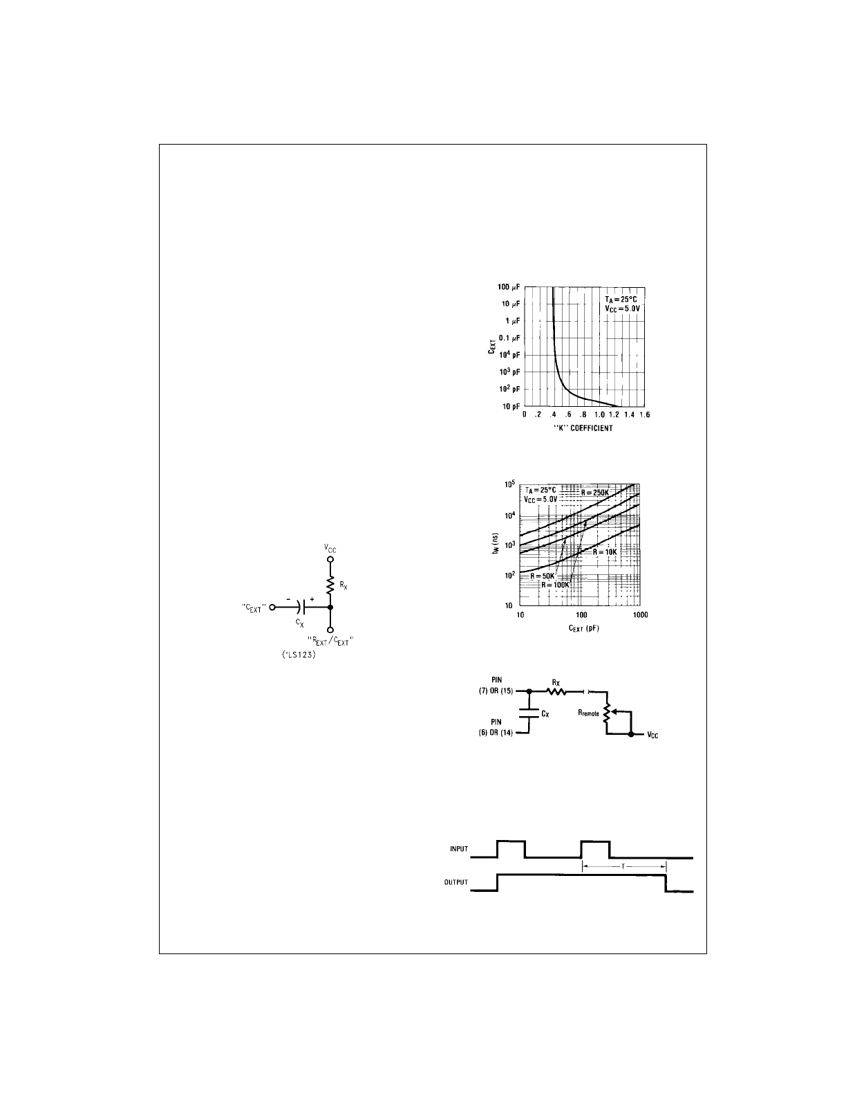
Operating Rules
1. An external resistor (R
X
) and an external capacitor (C
X
)
are required for proper operation. The value of C
X
may
vary from 0 to any necessary value. For small time con-
stants high-grade mica, glass, polypropylene, polycar-
bonate, or polystyrene material capacitors may be
used. For large time constants use tantalum or special
aluminum capacitors. If the timing capacitors have
leakages approaching 100 nA or if stray capacitance
from either terminal to ground is greater than 50 pF the
timing equations may not represent the pulse width the
device generates.
2. When an electrolytic capacitor is used for C
X
a switch-
ing diode is often required for standard TTL one-shots
to prevent high inverse leakage current. This switching
diode is not needed for the DM74LS123 one-shot and
should not be used. In general the use of the switching
diode is not recommended with retriggerable operation.
Furthermore, if a polarized timing capacitor is used on
the DM74LS123 the negative terminal of the capacitor
should be connected to the “C
EXT
” pin of the device
(Figure 1).
FIGURE 1.
3. For C
X
>>
1000 pF the output pulse width (t
W
) is
defined as follows:
t
W
=
KR
X
C
X
where [R
X
is in k
Ω
]
[C
X
is in pF]
[t
W
is in ns]
K
≈
0.37
4. The multiplicative factor K is plotted as a function of C
X
below for design considerations:
FIGURE 2.
5. For C
X
<
1000 pF see Figure 3 for t
W
vs. C
X
family
curves with R
X
as a parameter:
FIGURE 3.
6. To obtain variable pulse widths by remote trimming, the
following circuit is recommended:
FIGURE 4.
“R
remote
” should be as close to the device pin as possible.
7. The retriggerable pulse width is calculated as shown
below:
T
=
t
W
+
t
PLH
=
K
×
R
X
×
C
X
+
t
PLH
The retriggered pulse width is equal to the pulse width
plus a delay time period (Figure 5).
FIGURE 5.
3
www.fairchildsemi.com
DM74LS123
Operating Rules
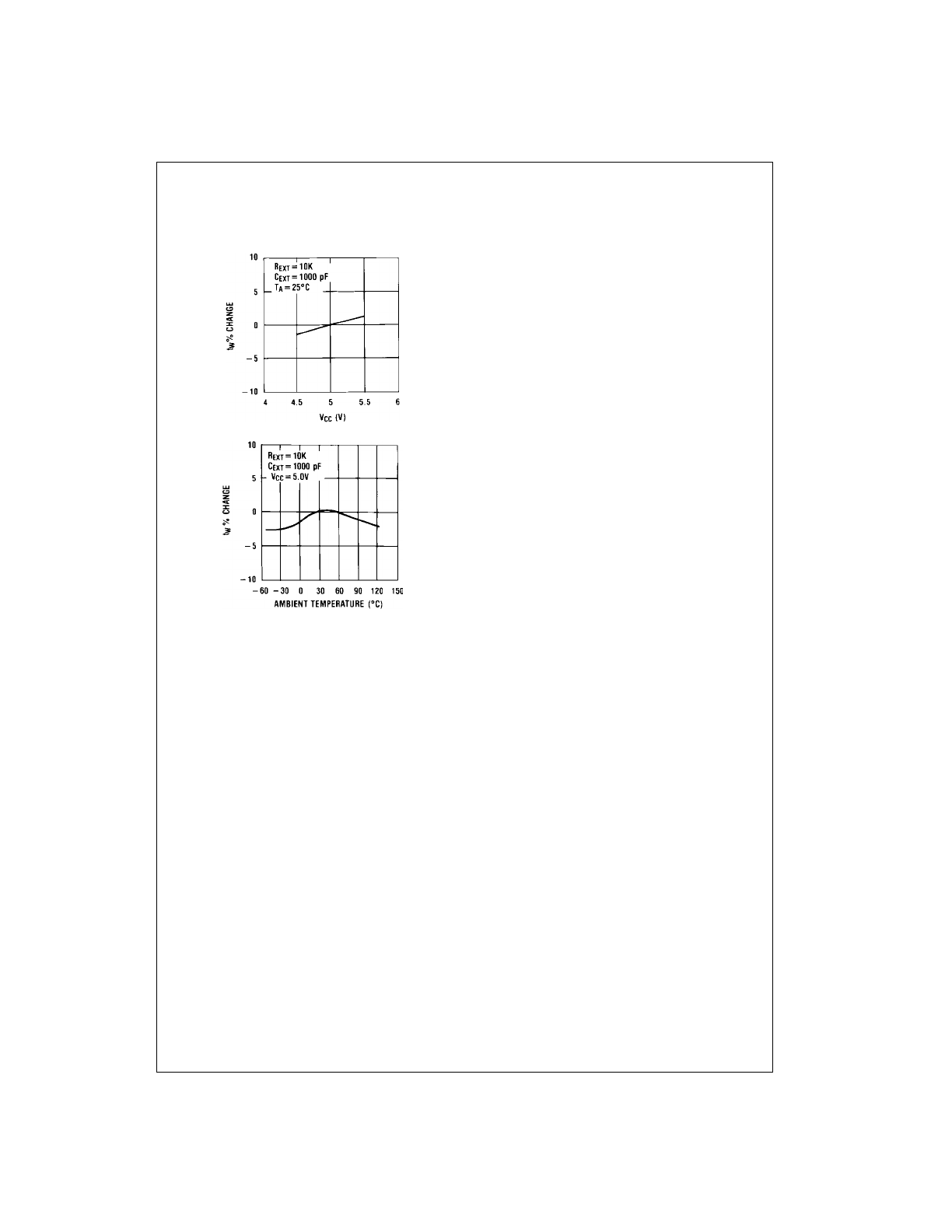
(Continued)
8. Output pulse width variation versus V
CC
and tempera-
tures: Figure 6 depicts the relationship between pulse
width variation versus V
CC
, and Figure 7 depicts pulse
width variation versus temperatures.
FIGURE 6.
FIGURE 7.
9. Under any operating condition C
X
and R
X
must be kept
as close to the one-shot device pins as possible to min-
imize stray capacitance, to reduce noise pick-up, and
to reduce I-R and Ldi/dt voltage developed along their
connecting paths. If the lead length from C
X
to pins (6)
and (7) or pins (14) and (15) is greater than 3 cm, for
example, the output pulse width might be quite different
from values predicted from the appropriate equations.
A non-inductive and low capacitive path is necessary to
ensure complete discharge of C
X
in each cycle of its
operation so that the output pulse width will be accu-
rate.
10. The C
EXT
pins of this device are internally connected to
the internal ground. For optimum system performance
they should be hard wired to the system’s return
ground plane.
11. V
CC
and ground wiring should conform to good high-
frequency standards and practices so that switching
transients on the V
CC
and ground return leads do not
cause interaction between one-shots. A 0.01
µ
F to 0.10
µ
F bypass capacitor (disk ceramic or monolithic type)
from V
CC
to ground is necessary on each device. Fur-
thermore, the bypass capacitor should be located as
close to the V
CC
-pin as space permits.
Note: For further detailed device characteristics and output per-
formance please refer to the Fairchild Semiconductor one-shot
application note AN-372.
www.fairchildsemi.com
4
DM74LS123
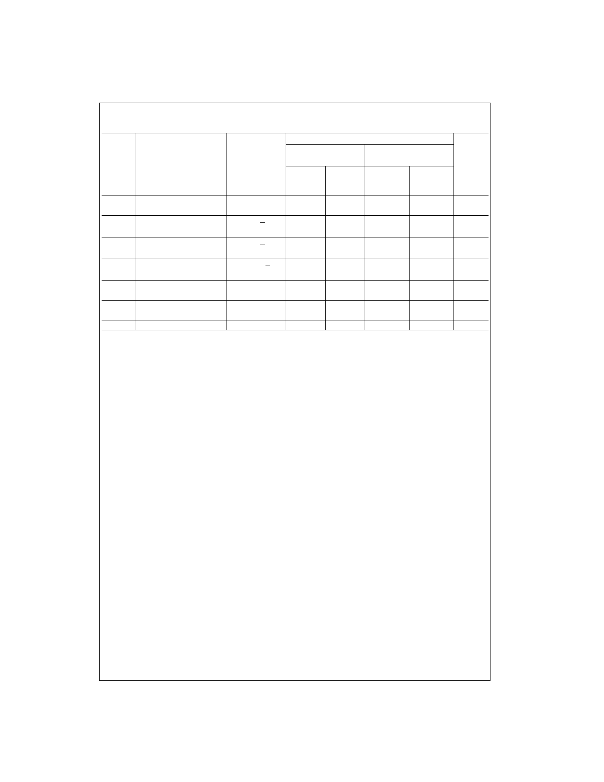
Absolute Maximum Ratings
(Note 1)
Note 1: The “Absolute Maximum Ratings” are those values beyond which
the safety of the device cannot be guaranteed. The device should not be
operated at these limits. The parametric values defined in the Electrical
Characteristics tables are not guaranteed at the absolute maximum ratings.
The “Recommended Operating Conditions” table will define the conditions
for actual device operation.
Recommended Operating Conditions
Note 2: T
A
=
25
°
C and V
CC
=
5V.
Electrical Characteristics
over recommended operating free air temperature range (unless otherwise noted)
Note 3: All typicals are at V
CC
=
5V, T
A
=
25
°
C.
Note 4: Not more than one output should be shorted at a time, and the duration should not exceed one second.
Note 5: Quiescent I
CC
is measured (after clearing) with 2.4V applied to all clear and A inputs, B inputs grounded, all outputs OPEN, C
EXT
=
0.02
µ
F,
and R
EXT
=
25 k
Ω
.
Note 6: I
CC
is measured in the triggered state with 2.4V applied to all clear and B inputs, A inputs grounded, all outputs OPEN, C
EXT
=
0.02
µ
F,
and R
EXT
=
25 k
Ω
.
Note 7: With all outputs OPEN and 4.5V applied to all data and clear inputs, I
CC
is measured after a momentary ground, then 4.5V is applied to the clock.
Supply Voltage
7V
Input Voltage
7V
Operating Free Air Temperature Range
0
°
C to
+
70
°
C
Storage Temperature
−
65
°
C to
+
150
°
C
Symbol
Parameter
Min
Nom
Max
Units
V
CC
Supply Voltage
4.75
5
5.25
V
V
IH
HIGH Level Input Voltage
2
V
V
IL
LOW Level Input Voltage
0.8
V
I
OH
HIGH Level Output Current
−
0.4
mA
I
OL
LOW Level Output Current
8
mA
t
W
Pulse Width
A or B HIGH
40
(Note 2)
A or B LOW
40
ns
Clear LOW
40
R
EXT
External Timing Resistor
5
260
k
Ω
C
EXT
External Timing Capacitance
No Restriction
µ
F
C
WIRE
Wiring Capacitance at R
EXT
/C
EXT
Terminal
50
pF
T
A
Free Air Operating Temperature
0
70
°
C
Symbol
Parameter
Conditions
Min
Typ
Max
Units
(Note 3)
V
I
Input Clamp Voltage
V
CC
=
Min, I
I
=
−
18 mA
−
1.5
V
V
OH
HIGH Level
V
CC
=
Min, I
OH
=
Max
2.7
3.4
V
Output Voltage
V
IL
=
Max, V
IH
=
Min
V
OL
LOW Level
V
CC
=
Min, I
OL
=
Max
0.35
0.5
Output Voltage
V
IL
=
Max, V
IH
=
Min
V
I
OL
=
4 mA, V
CC
=
Min
0.25
0.4
I
I
Input Current @ Max Input Voltage
V
CC
=
Max, V
I
=
7V
0.1
mA
I
IH
HIGH Level Input Current
V
CC
=
Max, V
I
=
2.7V
20
µ
A
I
IL
LOW Level Input Current
V
CC
=
Max, V
I
=
0.4V
−
0.4
mA
I
OS
Short Circuit Output Current
V
CC
=
Max (Note 4)
−
20
−
100
mA
I
CC
Supply Current
V
CC
=
Max (Note 5)(Note 6)(Note 7)
12
20
mA
5
www.fairchildsemi.com
DM74LS123
Switching Characteristics
at V
CC
=
5V and T
A
=
25
°
C
Symbol
Parameters
R
L
=
2 k
Ω
Units
From (Input)
C
L
=
15pF
C
L
=
15pF
To (Output)
C
EXT
=
0 pF, R
EXT
=
5 k
Ω
C
EXT
=
1000 pF, R
EXT
=
10 k
Ω
Min
Max
Min
Max
t
PLH
Propagation Delay Time
A to Q
33
ns
LOW-to-HIGH Level Output
t
PLH
Propagation Delay Time
B to Q
44
ns
LOW-to-HIGH Level Output
t
PHL
Propagation Delay Time
A to Q
45
ns
HIGH-to-LOW Level Output
t
PHL
Propagation Delay Time
B to Q
56
ns
HIGH-to-LOW Level Output
t
PLH
Propagation Delay Time
Clear to Q
45
ns
LOW-to-HIGH Level Output
t
PHL
Propagation Delay Time
Clear to Q
27
ns
HIGH-to-LOW Level Output
t
WQ(Min)
Minimum Width of Pulse
A or B to Q
200
ns
at Output Q
t
W(out)
Output Pulse Width
A or B to Q
4
5
µ
s
www.fairchildsemi.com
6
DM74LS123
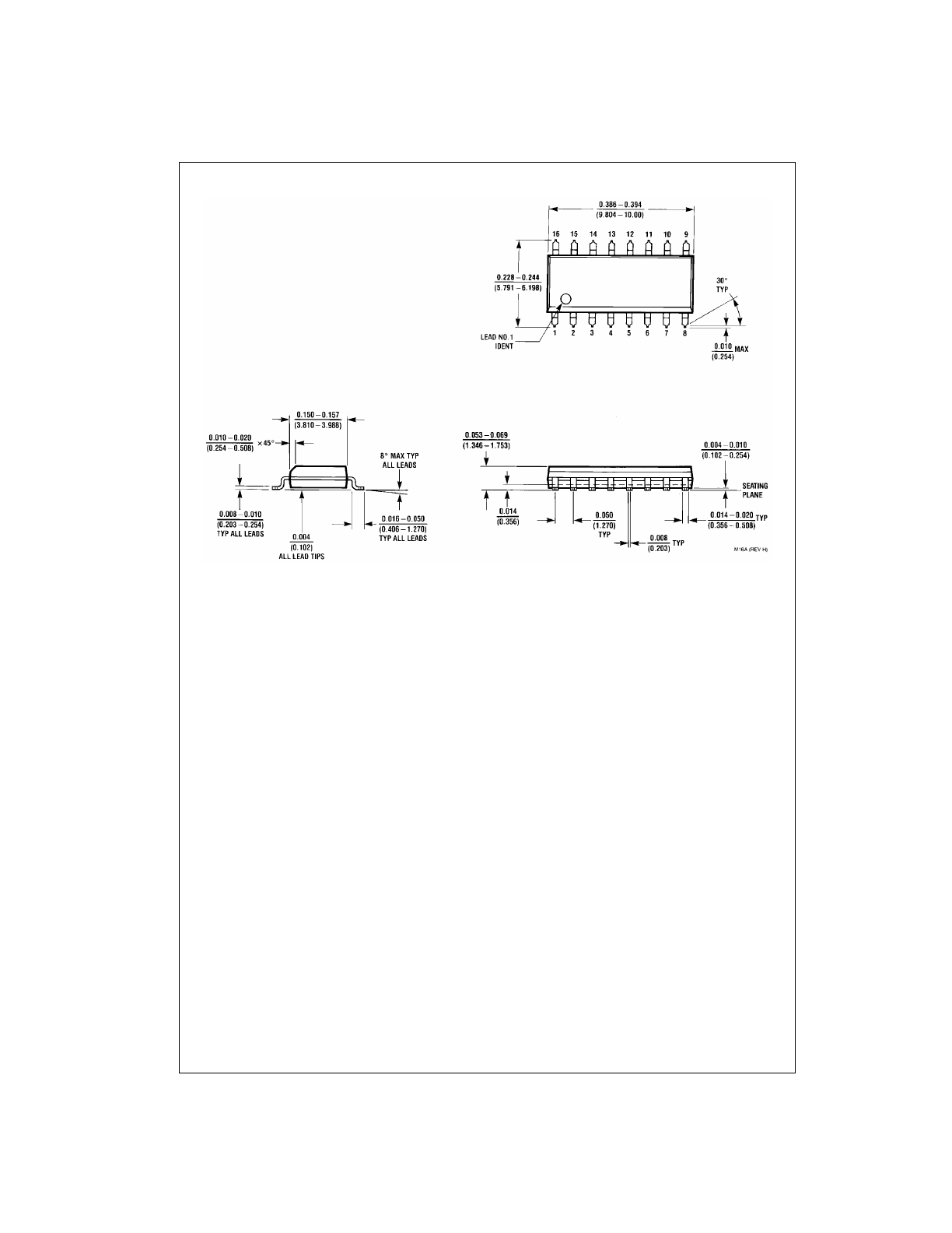
Physical Dimensions
inches (millimeters) unless otherwise noted
16-Lead Small Outline Integrated Circuit (SOIC), JEDEC MS-012, 0.150 Narrow
Package Number M16A
7
www.fairchildsemi.com
DM74LS123
Physical Dimensions
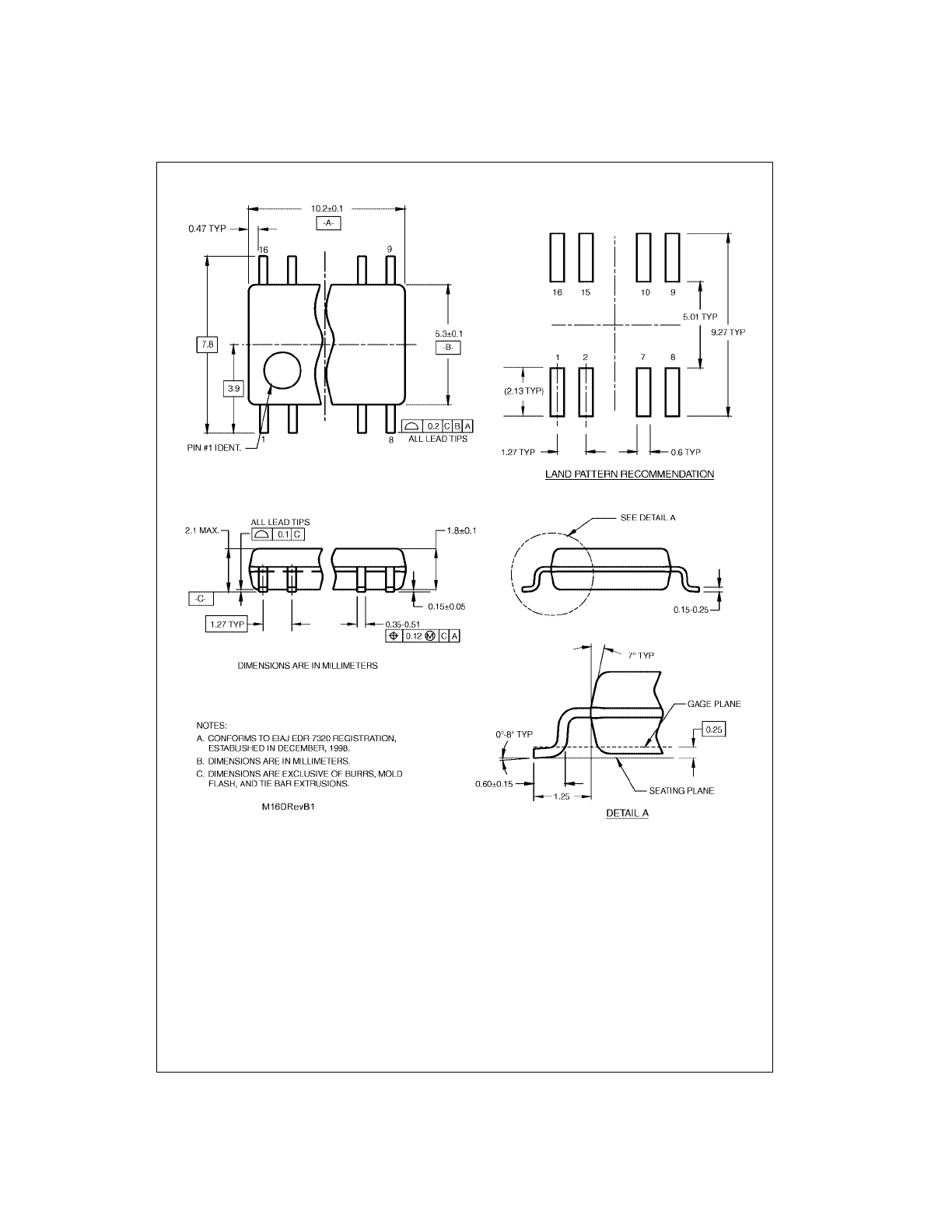
inches (millimeters) unless otherwise noted (Continued)
16-Lead Small Outline Package (SOP), EIAJ TYPE II, 5.3mm Wide
Package Number M16D
www.fairchildsemi.com
8
DM74LS123 Dual
Ret
ri
ggerabl
e O
ne-
Shot
wit
h
C
lear
and Com
p
le
mentar
y O
u
tputs
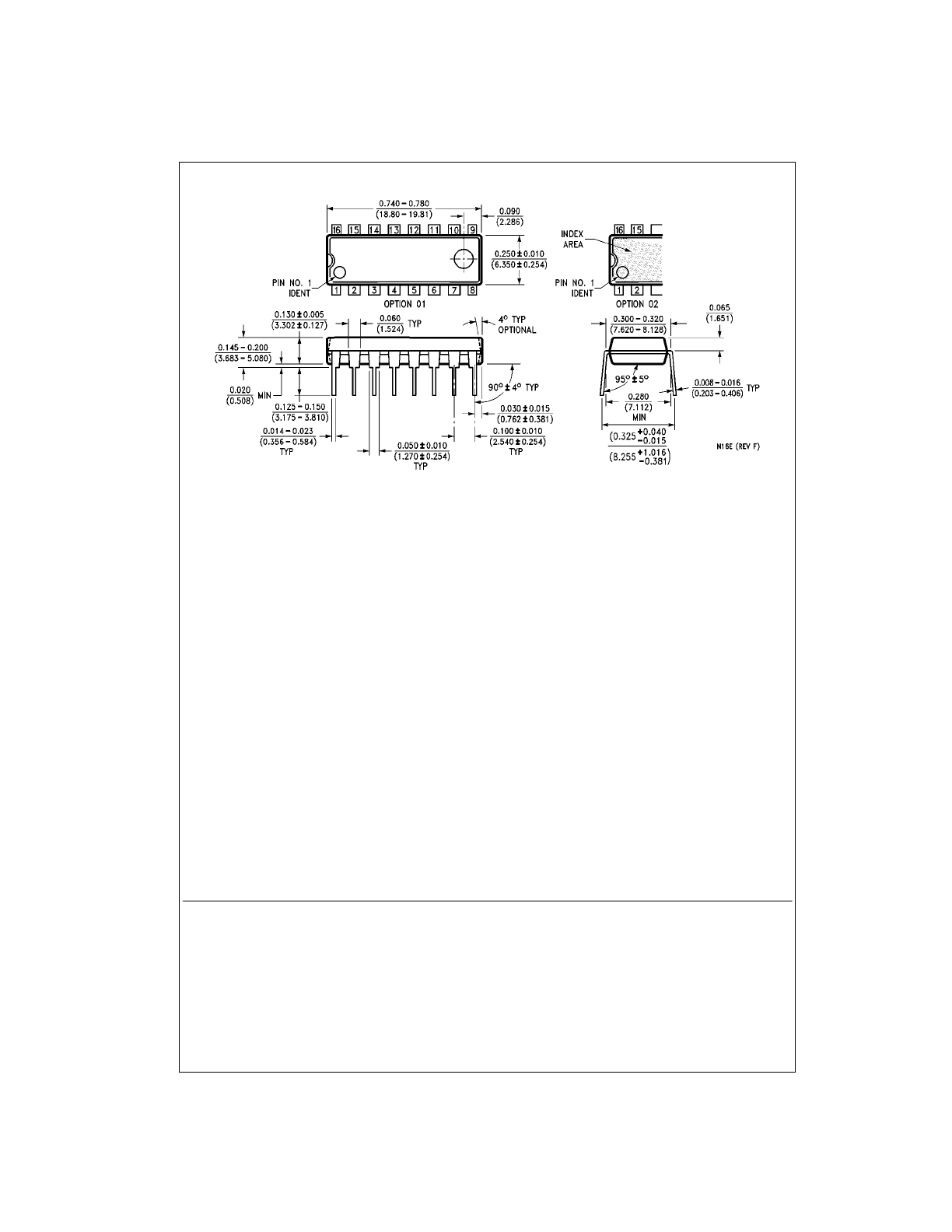
Physical Dimensions
inches (millimeters) unless otherwise noted (Continued)
16-Lead Plastic Dual-In-Line Package (PDIP), JEDEC MS-001, 0.300 Wide
Package Number N16E
Fairchild does not assume any responsibility for use of any circuitry described, no circuit patent licenses are implied and
Fairchild reserves the right at any time without notice to change said circuitry and specifications.
LIFE SUPPORT POLICY
FAIRCHILD’S PRODUCTS ARE NOT AUTHORIZED FOR USE AS CRITICAL COMPONENTS IN LIFE SUPPORT
DEVICES OR SYSTEMS WITHOUT THE EXPRESS WRITTEN APPROVAL OF THE PRESIDENT OF FAIRCHILD
SEMICONDUCTOR CORPORATION. As used herein:
1. Life support devices or systems are devices or systems
which, (a) are intended for surgical implant into the
body, or (b) support or sustain life, and (c) whose failure
to perform when properly used in accordance with
instructions for use provided in the labeling, can be rea-
sonably expected to result in a significant injury to the
user.
2. A critical component in any component of a life support
device or system whose failure to perform can be rea-
sonably expected to cause the failure of the life support
device or system, or to affect its safety or effectiveness.
www.fairchildsemi.com