
© 2000 Fairchild Semiconductor Corporation
DS006346
www.fairchildsemi.com
August 1986
Revised March 2000
DM74LS05 Hex Inver
ter
s
wi
th Open-Col
lec
tor
Outpu
ts
DM74LS05
Hex Inverters with Open-Collector Outputs
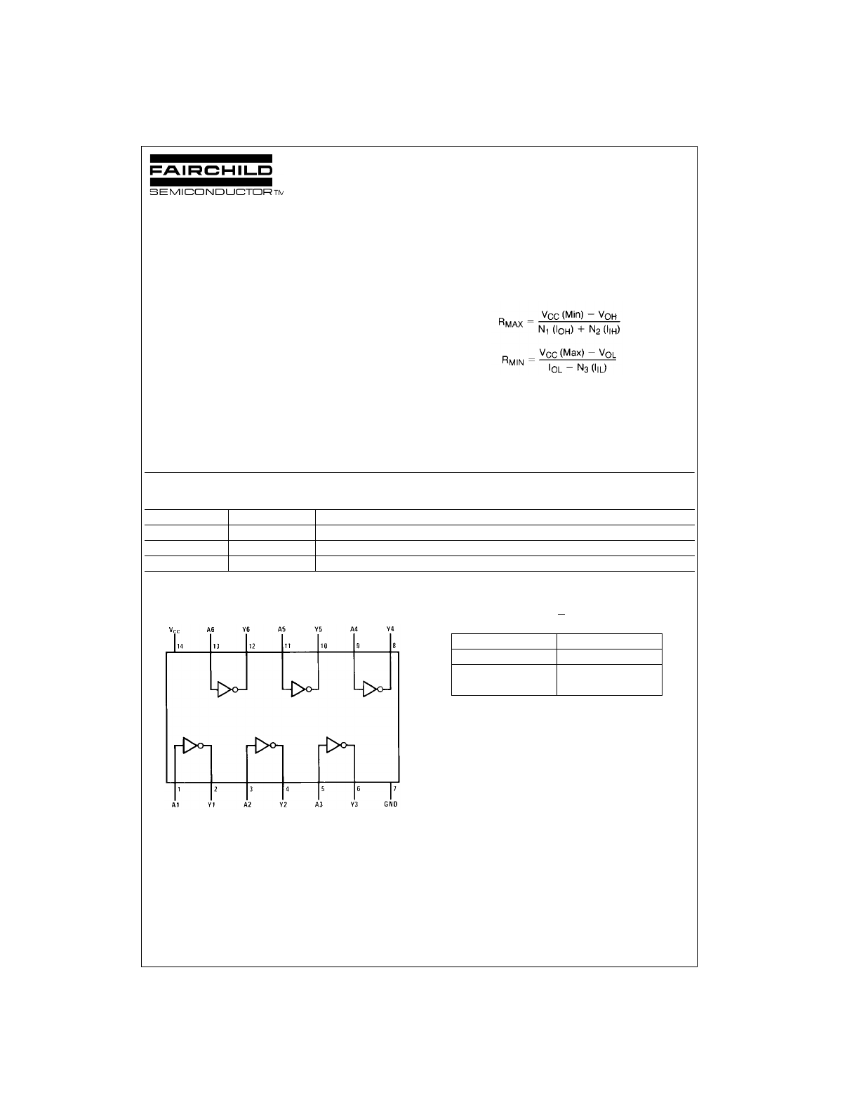
General Description
This device contains six independent gates each of which
performs the logic INVERT function. The open-collector
outputs require external pull-up resistors for proper logical
operation.
Pull-Up Resistor Equations
Where: N
1
(I
OH
)
=
total maximum output high current
for all outputs tied to pull-up resistor
N
2
(I
IH
)
=
total maximum input high current for
all inputs tied to pull-up resistor
N
3
(I
IL
)
=
total maximum input low current for
all inputs tied to pull-up resistor
Ordering Code:
Devices also available in Tape and Reel. Specify by appending the suffix letter “X” to the ordering code.
Connection Diagram
Function Table
Y
=
A
H
=
HIGH Logic Level
L
=
LOW Logic Level
Order Number
Package Number
Package Description
DM74LS05M
M14A
14-Lead Small Outline Integrated Circuit (SOIC), JEDEC MS-120, 0.150 Narrow
DM74LS05SJ
M14D
14-Lead Small Outline Package (SOP), EIAJ TYPE II, 5.3mm Wide
DM74LS05N
N14A
14-Lead Plastic Dual-In-Line Package (PDIP), JEDEC MS-001, 0.300 Wide
Input
Output
A
Y
L
H
H
L
www.fairchildsemi.com
2
D
M
74LS05
Absolute Maximum Ratings
(Note 1)
Note 1: The “Absolute Maximum Ratings” are those values beyond which
the safety of the device cannot be guaranteed. The device should not be
operated at these limits. The parametric values defined in the Electrical
Characteristics tables are not guaranteed at the absolute maximum ratings.
The “Recommended Operating Conditions” table will define the conditions
for actual device operation.
Recommended Operating Conditions
Electrical Characteristics
over recommended operating free air temperature range (unless otherwise noted)
Note 2: All typicals are at V
CC
=
5V, T
A
=
25
°
C.
Switching Characteristics
at V
CC
=
5V and T
A
=
25
°
C
Supply Voltage
7V
Input Voltage
7V
Output Voltage
7V
Operating Free Air Temperature Range
0
°
C to
+
70
°
C
Storage Temperature Range
−
65
°
C to
+
150
°
C
Symbol
Parameter
Min
Nom
Max
Units
V
CC
Supply Voltage
4.75
5
5.25
V
V
IH
HIGH Level Input Voltage
2
V
V
IL
LOW Level Input Voltage
0.8
V
V
OH
HIGH Level Output Voltage
5.5
V
I
OL
LOW Level Output Current
8
mA
T
A
Free Air Operating Temperature
0
70
°
C
Symbol
Parameter
Conditions
Min
Typ
Max
Units
(Note 2)
V
I
Input Clamp Voltage
V
CC
=
Min, I
I
=
−
18 mA
−
1.5
V
I
CEX
HIGH Level
V
CC
=
Min, V
O
=
5.5V
100
µ
A
Output Current
V
IL
=
Max
V
OL
LOW
Level V
CC
=
Min, I
OL
=
Max
0.35
0.5
Output Voltage
V
IH
=
Min
V
I
OL
=
4 mA, V
CC
=
Min
0.25
0.4
I
I
Input Current @ Max Input Voltage
V
CC
=
Max, V
I
=
7V
0.1
mA
I
IH
HIGH Level Input Current
V
CC
=
Max, V
I
=
2.7V
20
µ
A
I
IL
LOW Level Input Current
V
CC
=
Max, V
I
=
0.4V
−
0.36
mA
I
CCH
Supply Current with Outputs HIGH
V
CC
=
Max
1.2
2.4
mA
I
CCL
Supply Current with Outputs LOW
V
CC
=
Max
3.6
6.6
mA
R
L
=
2 k
Ω
Symbol
Parameter
C
L
=
15 pF
C
L
=
50 pF
Units
Min
Max
Min
Max
t
PLH
Propagation Delay Time
6
20
20
45
ns
LOW-to-HIGH Level Output
t
PHL
Propagation Delay Time
3
15
4
20
ns
HIGH-to-LOW Level Output
3
www.fairchildsemi.com
DM74LS05
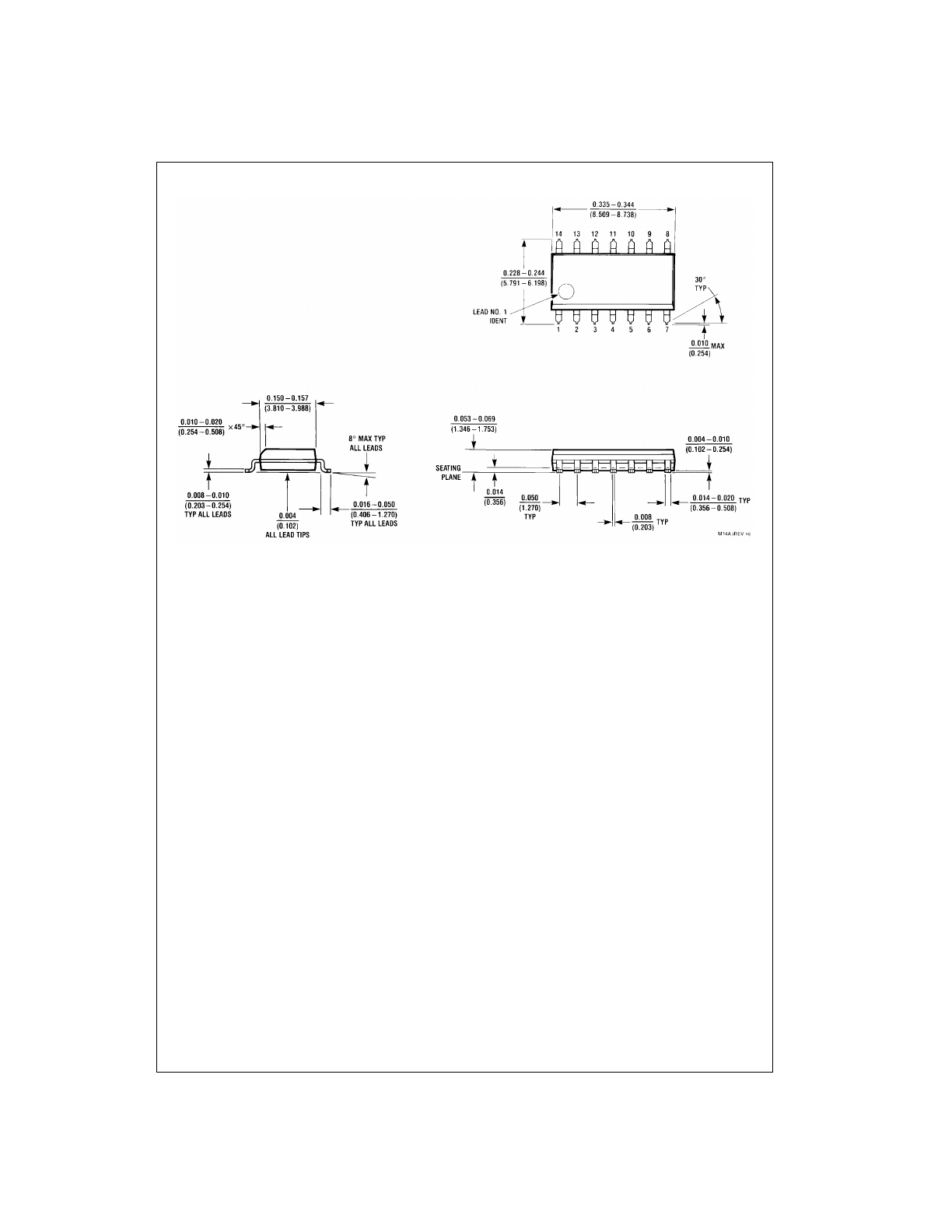
Physical Dimensions
inches (millimeters) unless otherwise noted
14-Lead Small Outline Integrated Circuit (SOIC), JEDEC MS-120, 0.150 Narrow
Package Number M14A
www.fairchildsemi.com
4
D
M
74LS05
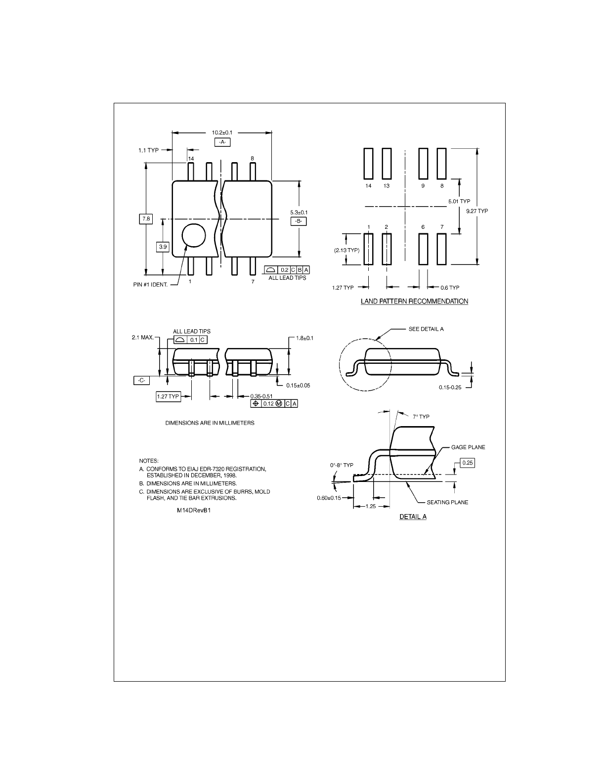
Physical Dimensions
inches (millimeters) unless otherwise noted (Continued)
14-Lead Small Outline Package (SOP), EIAJ TYPE II, 5.3mm Wide
Package Number M14D
5
www.fairchildsemi.com
DM74LS05 Hex Inver
ter
s
wi
th Open-Col
lec
tor
Outpu
ts
Physical Dimensions
inches (millimeters) unless otherwise noted (Continued)
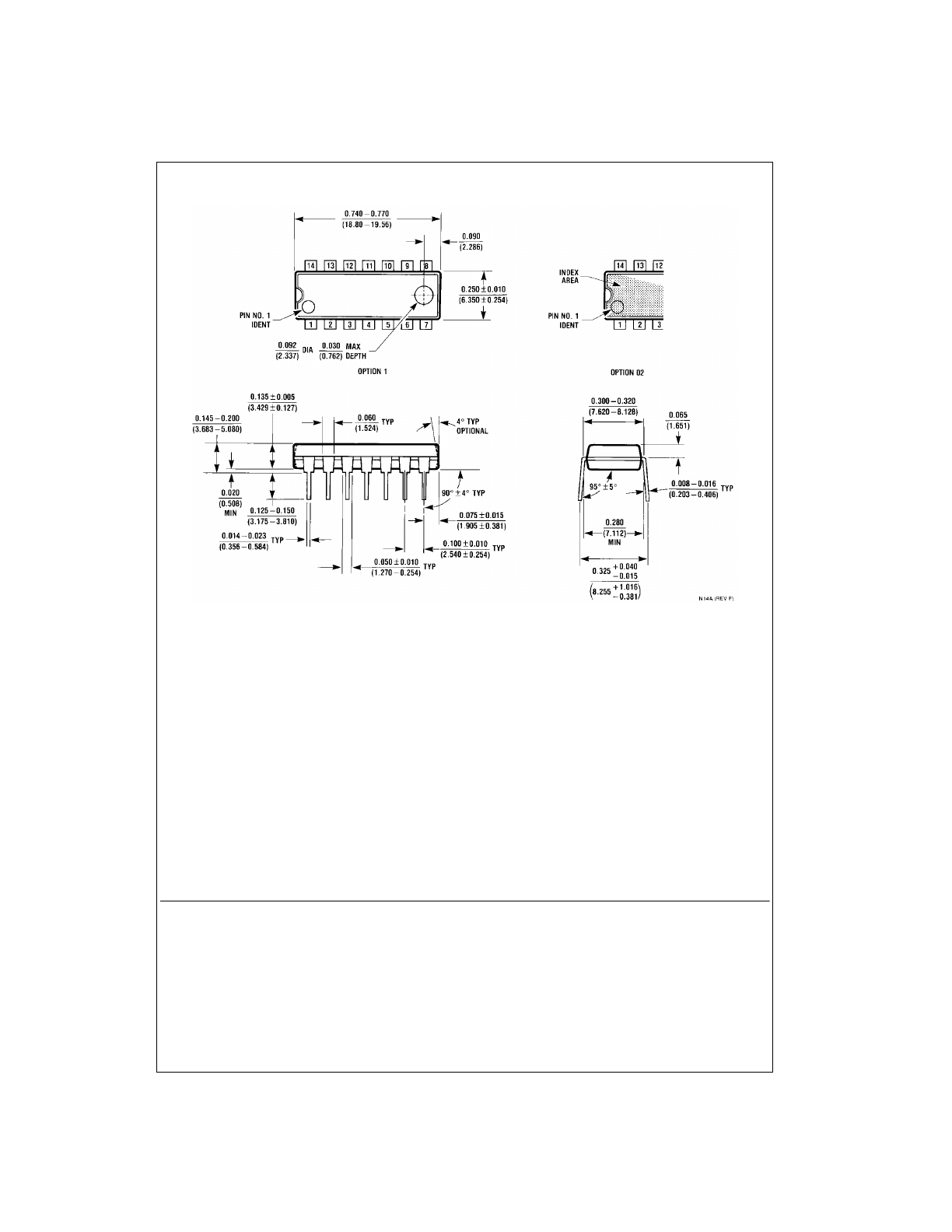
14-Lead Plastic Dual-In-Line Package (PDIP), JEDEC MS-001, 0.300 Wide
Package Number N14A
Fairchild does not assume any responsibility for use of any circuitry described, no circuit patent licenses are implied and
Fairchild reserves the right at any time without notice to change said circuitry and specifications.
LIFE SUPPORT POLICY
FAIRCHILD’S PRODUCTS ARE NOT AUTHORIZED FOR USE AS CRITICAL COMPONENTS IN LIFE SUPPORT
DEVICES OR SYSTEMS WITHOUT THE EXPRESS WRITTEN APPROVAL OF THE PRESIDENT OF FAIRCHILD
SEMICONDUCTOR CORPORATION. As used herein:
1. Life support devices or systems are devices or systems
which, (a) are intended for surgical implant into the
body, or (b) support or sustain life, and (c) whose failure
to perform when properly used in accordance with
instructions for use provided in the labeling, can be rea-
sonably expected to result in a significant injury to the
user.
2. A critical component in any component of a life support
device or system whose failure to perform can be rea-
sonably expected to cause the failure of the life support
device or system, or to affect its safety or effectiveness.
www.fairchildsemi.com