
TL/F/6356
54LS21/DM54LS21/DM74LS21
Dual
4-Input
AND
Gates
June 1989
54LS21/DM54LS21/DM74LS21 Dual 4-Input AND Gates
General Description
This device contains two independent gates each of which
performs the logic AND function.
Features
Y
Alternate Military/Aerospace device (54LS21) is avail-
able. Contact a National Semiconductor Sales Office/
Distributor for specifications.
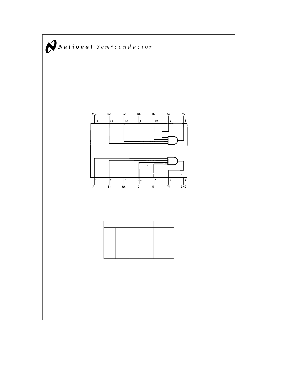
Connection Diagram
Dual-In-Line Package
TL/F/6356 – 1
Order Number 54LS21DMQB, 54LS21FMQB, 54LS21LMQB,
DM54LS21J, DM54LS21W, DM74LS21M or DM74LS21N
See NS Package Number E20A, J14A, M14A, N14A or W14B
Function Table
Y
e
ABCD
Inputs
Output
A
B
C
D
Y
X
X
X
L
L
X
X
L
X
L
X
L
X
X
L
L
X
X
X
L
H
H
H
H
H
H e High Logic Level
L e Low Logic Level
X e Either Low or High Logic Level
C1995 National Semiconductor Corporation
RRD-B30M105/Printed in U. S. A.
Absolute Maximum Ratings
(Note)
If Military/Aerospace specified devices are required,
please contact the National Semiconductor Sales
Office/Distributors for availability and specifications.
Supply Voltage
7V
Input Voltage
7V
Operating Free Air Temperature Range
DM54LS and 54LS
b
55
§
C to
a
125
§
C
DM74LS
0
§
C to
a
70
§
C
Storage Temperature Range
b
65
§
C to
a
150
§
C
Note:
The ‘‘Absolute Maximum Ratings’’ are those values
beyond which the safety of the device cannot be guaran-
teed. The device should not be operated at these limits. The
parametric values defined in the ‘‘Electrical Characteristics’’
table are not guaranteed at the absolute maximum ratings.
The ‘‘Recommended Operating Conditions’’ table will define
the conditions for actual device operation.
Recommended Operating Conditions
Symbol
Parameter
DM54LS21
DM74LS21
Units
Min
Nom
Max
Min
Nom
Max
V
CC
Supply Voltage
4.5
5
5.5
4.75
5
5.25
V
V
IH
High Level Input Voltage
2
2
V
V
IL
Low Level Input Voltage
0.7
0.8
V
I
OH
High Level Output Current
b
0.4
b
0.4
mA
I
OL
Low Level Output Current
4
8
mA
T
A
Free Air Operating Temperature
b
55
125
0
70
§
C
Electrical Characteristics
over recommended operating free air temperature range (unless otherwise noted)
Symbol
Parameter
Conditions
Min
Typ
Max
Units
(Note 1)
V
I
Input Clamp Voltage
V
CC
e
Min, I
I
e b
18 mA
b
1.5
V
V
OH
High Level Output
V
CC
e
Min, I
OH
e
Max,
DM54
2.5
3.4
V
Voltage
V
IH
e
Min
DM74
2.7
3.4
V
OL
Low Level Output
V
CC
e
Min, I
OL
e
Max,
DM54
0.25
0.4
Voltage
V
IL
e
Max
DM74
0.35
0.5
V
I
OL
e
4 mA, V
CC
e
Min
DM74
0.25
0.4
I
I
Input Current
@
Max
V
CC
e
Max, V
I
e
7V
0.1
mA
Input Voltage
I
IH
High Level Input Current
V
CC
e
Max, V
I
e
2.7V
20
m
A
I
IL
Low Level Input Current
V
CC
e
Max, V
I
e
0.4V
b
0.36
mA
I
OS
Short Circuit
V
CC
e
Max
DM54
b
20
b
100
mA
Output Current
(Note 2)
DM74
b
20
b
100
I
CCH
Supply Current with
V
CC
e
Max
1.2
2.4
mA
Outputs High
I
CCL
Supply Current with
V
CC
e
Max
2.2
4.4
mA
Outputs Low
Switching Characteristics
at V
CC
e
5V and T
A
e
25
§
C (See Section 1 for Test Waveforms and Output Load)
R
L
e
2 kX
Symbol
Parameter
C
L
e
15 pF
C
L
e
50 pF
Units
Min
Max
Min
Max
t
PLH
Propagation Delay Time
4
13
6
18
ns
Low to High Level Output
t
PHL
Propagation Delay Time
3
11
5
18
ns
High to Low Level Output
Note 1:
All typicals are at V
CC
e
5V, T
A
e
25
§
C.
Note 2:
Not more than one output should be shorted at a time, and the duration should not exceed one second.
2
3
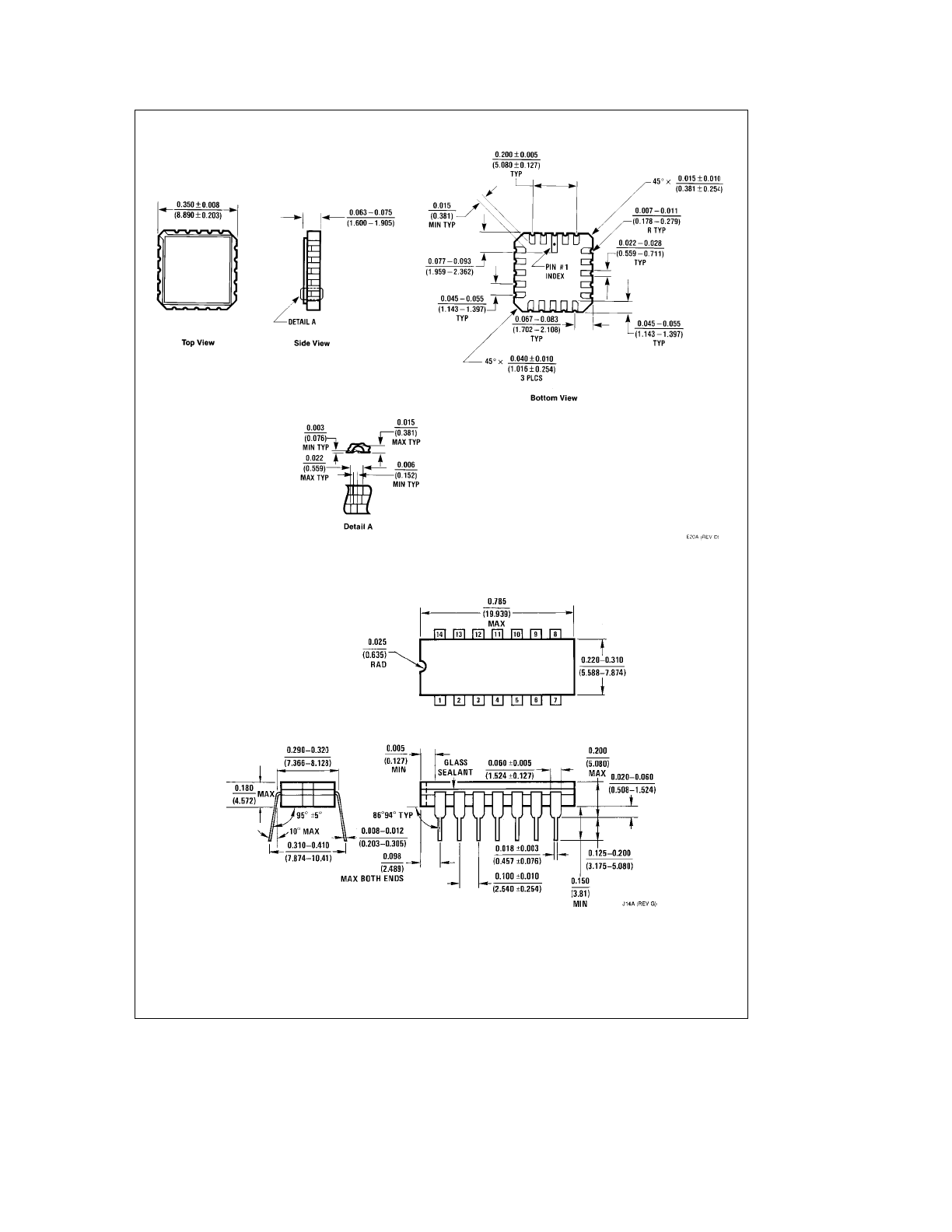
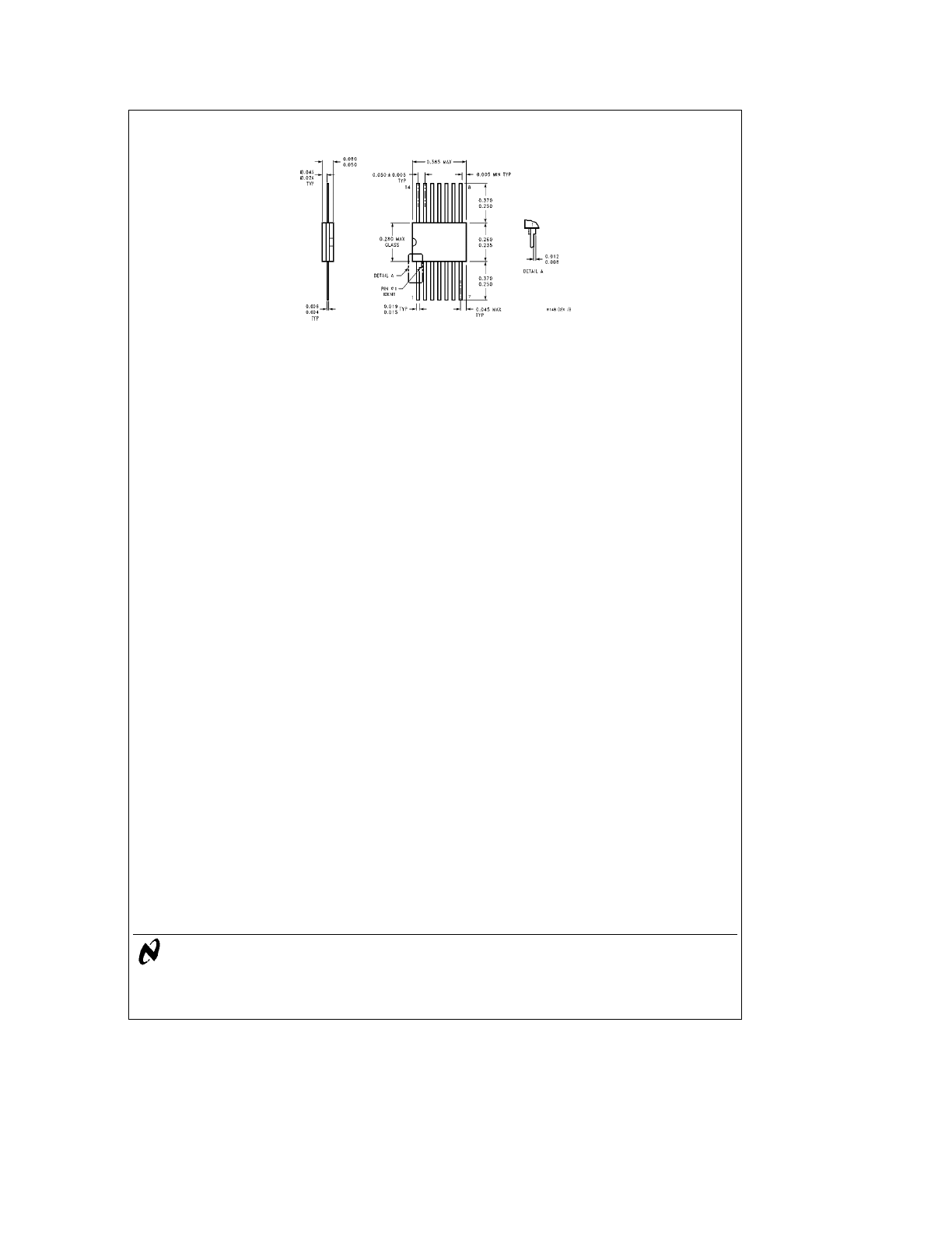
Physical Dimensions
inches (millimeters)
Ceramic Leadless Chip Carrier Package (E)
Order Number 54LS20LMQB
NS Package Number E20A
14-Lead Ceramic Dual-In-Line Package (J)
Order Number 54LS20DMQB or DM54LS21J
NS Package Number J14A
4
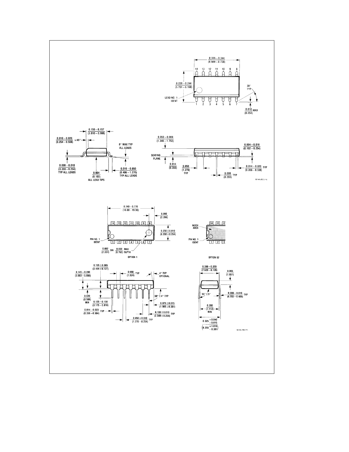
Physical Dimensions
inches (millimeters) (Continued)
14-Lead Small Outline Molded Package (M)
Order Number DM74LS21M
NS Package Number M14A
14-Lead Molded Dual-In-Line Package (N)
Order Number DM74LS21N
NS Package Number N14A
5
54LS21/DM54LS21/DM74LS21
Dual
4-Input
AND
Gates
Physical Dimensions
inches (millimeters) (Continued)
14-Lead Ceramic Flat Package (W)
Order Number 54LS21FMQB or DM54LS21W
NS Package Number W14B
LIFE SUPPORT POLICY
NATIONAL’S PRODUCTS ARE NOT AUTHORIZED FOR USE AS CRITICAL COMPONENTS IN LIFE SUPPORT
DEVICES OR SYSTEMS WITHOUT THE EXPRESS WRITTEN APPROVAL OF THE PRESIDENT OF NATIONAL
SEMICONDUCTOR CORPORATION. As used herein:
1. Life support devices or systems are devices or
2. A critical component is any component of a life
systems which, (a) are intended for surgical implant
support device or system whose failure to perform can
into the body, or (b) support or sustain life, and whose
be reasonably expected to cause the failure of the life
failure to perform, when properly used in accordance
support device or system, or to affect its safety or
with instructions for use provided in the labeling, can
effectiveness.
be reasonably expected to result in a significant injury
to the user.
National Semiconductor
National Semiconductor
National Semiconductor
National Semiconductor
Corporation
Europe
Hong Kong Ltd.
Japan Ltd.
1111 West Bardin Road
Fax: (
a
49) 0-180-530 85 86
13th Floor, Straight Block,
Tel: 81-043-299-2309
Arlington, TX 76017
Email: cnjwge
@
tevm2.nsc.com
Ocean Centre, 5 Canton Rd.
Fax: 81-043-299-2408
Tel: 1(800) 272-9959
Deutsch Tel: (
a
49) 0-180-530 85 85
Tsimshatsui, Kowloon
Fax: 1(800) 737-7018
English
Tel: (
a
49) 0-180-532 78 32
Hong Kong
Fran
3ais Tel: (
a
49) 0-180-532 93 58
Tel: (852) 2737-1600
Italiano
Tel: (
a
49) 0-180-534 16 80
Fax: (852) 2736-9960
National does not assume any responsibility for use of any circuitry described, no circuit patent licenses are implied and National reserves the right at any time without notice to change said circuitry and specifications.