
REV. 0
Information furnished by Analog Devices is believed to be accurate and
reliable. However, no responsibility is assumed by Analog Devices for its
use, nor for any infringements of patents or other rights of third parties
which may result from its use. No license is granted by implication or
otherwise under any patent or patent rights of Analog Devices.
a
EMI/EMC Compliant,
615 kV ESD Protected,
RS-232 Line Drivers/Receivers
ADM202E/ADM1181A
© Analog Devices, Inc., 1996
One Technology Way, P.O. Box 9106, Norwood, MA 02062-9106, U.S.A.
Tel: 617/329-4700
Fax: 617/326-8703
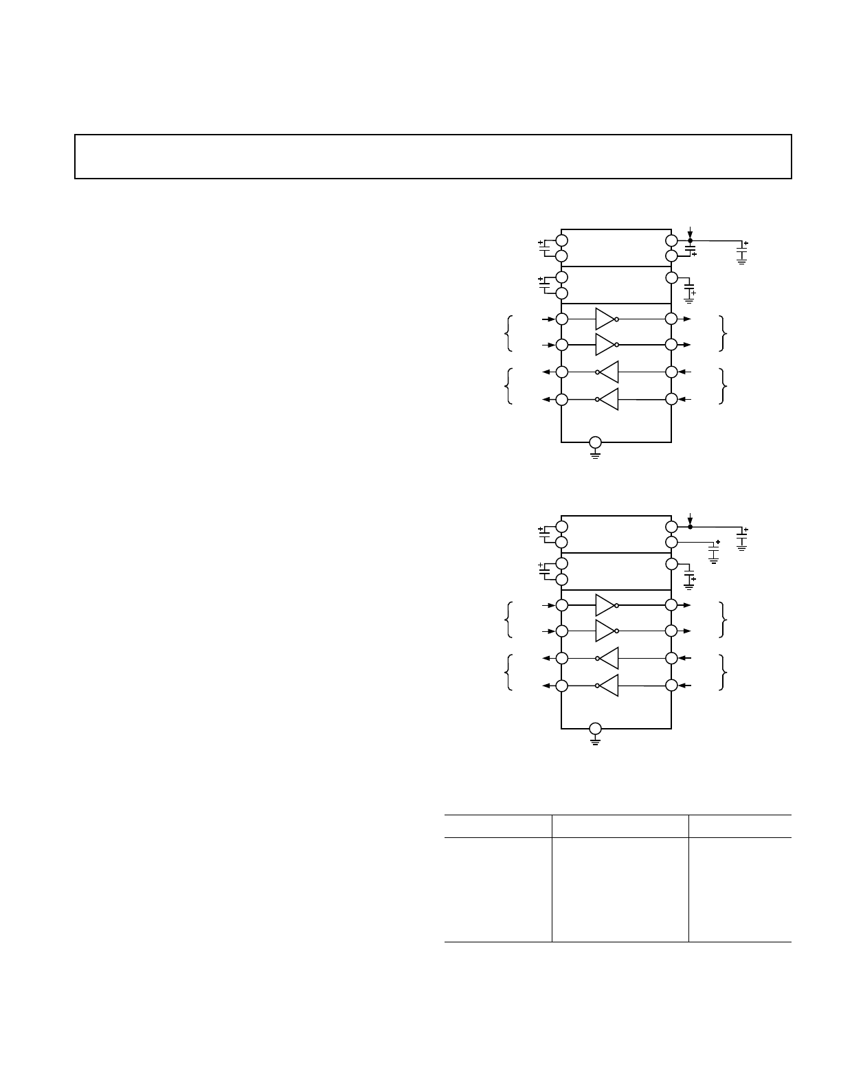
FUNCTIONAL BLOCK DIAGRAMS
C1+
C1–
C2+
C2–
V
CC
0.1µF
10V
0.1µF
10V
V+
V–
+5V TO +10V
VOLTAGE
DOUBLER
3
1
2
+5V INPUT
C3
0.1µF
10V
4
5
+10V TO –10V
VOLTAGE
INVERTER
6
C4
0.1µF
10V
14
11
T1
OUT
T1
IN
16
C5
0.1µF
10V
7
10
T2
OUT
T2
IN
12
13
8
9
ADM1181A
R1
OUT
R2
OUT
R1
IN
R2
IN
CMOS
INPUTS
CMOS
OUTPUTS
EIA/TIA-232
OUTPUTS
EIA/TIA-232
INPUTS
*
15
NOTE
*
INTERNAL 5k
Ω
PULL-DOWN RESISTOR ON EACH RS-232 INPUT
GND
C1+
C1–
C2+
C2–
V
CC
0.1µF
10V
0.1µF
10V
V+
V–
+5V TO +10V
VOLTAGE
DOUBLER
3
1
2
+5V INPUT
C3
0.1µF
6.3V
4
5
+10V TO –10V
VOLTAGE
INVERTER
6
C4
0.1µF
10V
14
11
T1
OUT
T1
IN
16
C5
0.1µF
7
10
T2
OUT
T2
IN
12
13
8
9
ADM202E
R1
OUT
R2
OUT
R1
IN
R2
IN
CMOS
INPUTS
CMOS
OUTPUTS
EIA/TIA-232
OUTPUTS
EIA/TIA-232
INPUTS
*
15
NOTE
*
INTERNAL 5k
Ω
PULL-DOWN RESISTOR ON EACH RS-232 INPUT
GND
T1
T2
R1
R2
T1
T2
R1
R2
GENERAL DESCRIPTION
The ADM202E and ADM1181A are robust, high speed, 2-
channel RS232/V.28 interface devices that operate from a single
+5 V power supply. Both products are suitable for operation in
harsh electrical environments and are compliant with the EU di-
rective on EMC (89/336/EEC). Both the level of electromag-
netic emissions and immunity are in compliance. EM immunity
includes ESD protection in excess of
±
15 kV on all I/O lines,
Fast Transient burst protection (1000-4-4) and Radiated Im-
munity (1000-4-3). EM emissions include radiated and
conducted emissions as required by Information Technology
Equipment EN55022, CISPR22.
The ADM202E and ADM1181A conform to the EIA-232E and
CCITT V.28 specifications and operate at data rates up to
230 kbps.
Four external 0.1
µ
F charge pump capacitors are used for the
voltage doubler/inverter permitting operation from a single +5 V
supply.
The ADM202E provides a robust pin-compatible upgrade for
existing ADM202, ADM232L or MAX202E/MAX232E sock-
ets. It is available in a 16-pin DIP, wide and narrow SO and also
a space saving TSSOP package. The TSSOP package gives a
44% space saving over SOIC.
The ADM1181A provides a robust pin compatible upgrade for
the LTC1181A, and it is available in 16-pin DIP and 16-lead
SO packages.
FEATURES
Complies with 89/336/EEC EMC Directive
ESD Protection to IEC1000-4-2 (801.2)
68 kV: Contact Discharge
615 kV: Air-Gap Discharge
615 kV: Human Body Model
EFT Fast Transient Burst Immunity (IEC1000-4-4)
Low EMI Emissions (EN55022)
230 kbits/s Data Rate Guaranteed
TSSOP Package Option
Upgrade for MAX202E, 232E, LT1181A
APPLICATIONS
General Purpose RS-232 Data Link
Portable Instruments
PDAs
ORDERING GUIDE
Model
Temperature Range
Package Option
ADM202EAN
–40
°
C to +85
°
C
N-16
ADM202EARW
–40
°
C to +85
°
C
R-16W
ADM202EARN
–40
°
C to +85
°
C
R-16N
ADM202EARU
–40
°
C to +85
°
C
RU-16
ADM1181AAN
–40
°
C to +85
°
C
N-16
ADM1181AARW
–40
°
C to +85
°
C
R-16W

REV. 0
–2–
ADM202E/ADM1181A–SPECIFICATIONS
(V
CC
= +5.0 V
6 10%, C1–C4 = 0.1 mF. All specifications
T
MIN
to T
MAX
unless otherwise noted.)
Parameter
Min
Typ
Max
Units
Test Conditions/Comments
DC CHARACTERISTICS
Operating Voltage Range
4.5
5.0
5.5
Volts
V
CC
Power Supply Current
2.0
3.0
mA
No Load
15
18
mA
R
L
= 3 k
Ω
to GND
LOGIC
Input Logic Threshold Low, V
INL
0.8
V
T
IN
Input Logic Threshold High, V
INH
2.4
V
T
IN
CMOS Output Voltage Low, V
OL
0.4
V
I
OUT
= 3.2 mA
CMOS Output Voltage High, V
OH
3.5
V
I
OUT
= –1 mA
Input Leakage Current
0.01
±
10
µ
A
T
IN
= GND to V
CC
RS-232 RECEIVER
EIA-232 Input Voltage Range
–30
+30
V
EIA-232 Input Threshold Low
0.4
0.8
V
EIA-232 Input Threshold High
1.1
2.4
V
EIA-232 Input Hysteresis
0.7
V
EIA-232 Input Resistance
3
5
7
k
Ω
RS-232 TRANSMITTER
Output Voltage Swing
±
5.0
±
9.0
Volts
All Transmitter Outputs
Loaded with 3 k
Ω
to Ground
Transmitter Output Resistance
300
Ω
V
CC
= 0 V, V
OUT
=
±
2 V
RS-232 Output Short Circuit Current
±
15
±
60
mA
TIMING CHARACTERISTICS
Maximum Data Rate
230
kbps
R
L
= 3 k
Ω
to 7 k
Ω
, C
L
= 50 pF to 2500 pF
Receiver Propagation Delay
TPHL
0.3
1
µ
s
TPLH
0.6
1
µ
s
Transmitter Propagation Delay
1.2
1.5
µ
s
R
L
= 3 k
Ω
, C
L
= 2500 pF
Transition Region Slew Rate
3
10
30
V/
µ
s
R
L
= 3 k
Ω
, C
L
= 2500 pF
Measured from +3 V to –3 V or
–3 V to +3 V
EM IMMUNITTY
ESD Protection (I/O pins)
±
15
kV
Human Body Model
±
15
kV
IEC1000-4-2 Air Discharge
±
8 kV
kV
IEC1000-4-2 Contact Discharge
EFT Protection (I/O pins)
±
2
kV
IEC1000-4-4
EMI Immunity
10
V/m
IEC1000-4-3
Specifications subject to change without notice.
ABSOLUTE MAXIMUM RATINGS*
(T
A
= +25
°
C unless otherwise noted)
V
CC
. . . . . . . . . . . . . . . . . . . . . . . . . . . . . . . . . . –0.3 V to +6 V
V+ . . . . . . . . . . . . . . . . . . . . . . . . . . . . (V
CC
– 0.3 V) to +14 V
V– . . . . . . . . . . . . . . . . . . . . . . . . . . . . . . . . . . +0.3 V to –14 V
Input Voltages
T
IN
. . . . . . . . . . . . . . . . . . . . . . . . . . –0.3 V to (V+, +0.3 V)
R
IN
. . . . . . . . . . . . . . . . . . . . . . . . . . . . . . . . . . . . . . .
±
30 V
Output Voltages
T
OUT
. . . . . . . . . . . . . . . . . . . . . . . . . . . . . . . . . . . . .
±
15 V
R
OUT
. . . . . . . . . . . . . . . . . . . . . . . . –0.3 V to (V
CC
+ 0.3 V)
Short Circuit Duration
T
OUT
. . . . . . . . . . . . . . . . . . . . . . . . . . . . . . . . . Continuous
Power Dissipation
Power Dissipation N-16 . . . . . . . . . . . . . . . . . . . . . . . . 450 mW
(Derate 6 mW/
°
C above +50
°
C)
θ
JA
, Thermal Impedance . . . . . . . . . . . . . . . . . . . . . 117
°
C/W
Power Dissipation R-16 . . . . . . . . . . . . . . . . . . . . . . . . 450 mW
(Derate 6 mW/
°
C above +50
°
C)
θ
JA
, Thermal Impedance . . . . . . . . . . . . . . . . . . . . . 158
°
C/W
Power Dissipation RU-16 . . . . . . . . . . . . . . . . . . . . . . 500 mW
(Derate 6 mW/
°
C above +50
°
C)
θ
JA
, Thermal Impedance . . . . . . . . . . . . . . . . . . . . . 158
°
C/W
Operating Temperature Range
Industrial (A Version) . . . . . . . . . . . . . . . . . –40
°
C to +85
°
C
Storage Temperature Range . . . . . . . . . . . . . –65
°
C to +150
°
C
Lead Temperature (Soldering, 10 sec) . . . . . . . . . . . . . +300
°
C
ESD Rating (MIL-STD-883B) (I/O Pins) . . . . . . . . . .
±
15 kV
ESD Rating MIL-STD-883B (Except I/O) . . . . . . . . . .
±
3 kV
ESD Rating (IEC1000-4-2 Air) (I/O Pins) . . . . . . . . .
±
15 kV
ESD Rating (IEC1000-4-2 Contact) (I/O Pins) . . . . . . .
±
8 kV
EFT Rating (IEC1000-4-4) (I/O Pins) . . . . . . . . . . . . .
±
2 kV
*This is a stress rating only and functional operation of the device at these or any
other conditions above those indicated in the operation sections of this specifica-
tion is not implied. Exposure to absolute maximum rating conditions for extended
periods of time may affect reliability.
ADM202E/ADM1181A
–3–
REV. 0
PIN FUNCTION DESCRIPTION
Mnemonic
Function
V
CC
Power Supply Input: +5 V
±
10%.
V+
Internally Generated Positive Supply
(+9 V nominal).
V–
Internally Generated Negative Supply
(–9 V nominal).
GND
Ground Pin. Must Be Connected to 0 V.
C1+, C1–
External Capacitor 1 is connected between
these pins. 0.1
µ
F capacitor is recommended
but larger capacitors up to 47
µ
F may be used.
C2+, C2–
External Capacitor 2 is connected between
these pins. 0.1
µ
F capacitor is recommended
but larger capacitors up to 47
µ
F may be used.
T
IN
Transmitter (Driver) Inputs. These inputs ac-
cept TTL/CMOS levels.
T
OUT
Transmitter (Driver) Outputs. These are RS-
232 signal levels (typically
±
9 V).
R
IN
Receiver Inputs. These inputs accept RS-232
signal levels. An Internal 5 k
Ω
pull-down resis-
tor to GND is connected on each input.
R
OUT
Receiver Outputs. These are CMOS output
logic levels.
C1+
C1–
C2+
C2–
V
CC
0.1µF
10V
0.1µF
10V
V+
V–
+5V TO +10V
VOLTAGE
DOUBLER
3
1
2
+5V INPUT
C3
0.1µF
6.3V
4
5
+10V TO –10V
VOLTAGE
INVERTER
6
C4
0.1µF
10V
T1
14
11
T1
OUT
T1
IN
16
C5
0.1µF
7
10
T2
OUT
T2
IN
T2
12
13
8
9
R1
R2
ADM202E
R1
OUT
R2
OUT
R1
IN
R2
IN
CMOS
INPUTS
CMOS
OUTPUTS
EIA/TIA-232
OUTPUTS
EIA/TIA-232
INPUTS
*
15
NOTE
*
INTERNAL 5k
Ω
PULL-DOWN RESISTOR ON EACH RS-232 INPUT
GND
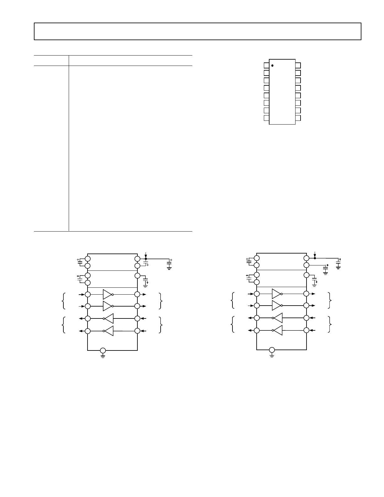
ADM202E Typical Operating Circuit
C1+
C1–
C2+
C2–
V
CC
0.1µF
10V
0.1µF
10V
V+
V–
+5V TO +10V
VOLTAGE
DOUBLER
3
1
2
+5V INPUT
C3
0.1µF
10V
4
5
+10V TO –10V
VOLTAGE
INVERTER
6
C4
0.1µF
10V
T1
14
11
T1
OUT
T1
IN
16
C5
0.1µF
10V
7
10
T2
OUT
T2
IN
T2
12
13
8
9
R1
R2
ADM1181A
R1
OUT
R2
OUT
R1
IN
R2
IN
CMOS
INPUTS
CMOS
OUTPUTS
EIA/TIA-232
OUTPUTS
EIA/TIA-232
INPUTS
*
15
NOTE
*
INTERNAL 5k
Ω
PULL-DOWN RESISTOR ON EACH RS-232 INPUT
GND
ADM1181A Typical Operating Circuit
PIN CONNECTIONS
14
13
12
11
16
15
10
9
8
1
2
3
4
7
6
5
TOP VIEW
(Not to Scale)
ADM202E
ADM1181A
NC = NO CONNECT
C1+
R1
IN
T1
OUT
GND
V
CC
V+
C1–
C2+
T2
IN
T1
IN
R1
OUT
C2–
V–
T2
OUT
R2
IN
R2
OUT
ADM202E/ADM1181A
–4–
REV. 0
GENERAL DESCRIPTION
The ADM202E/ADM1181E are ruggedized RS-232 line drivers/
receivers. Step-up voltage converters coupled with level shifting
transmitters and receivers allow RS-232 levels to be developed
while operating from a single +5 V supply.
Features include low power consumption, high transmission
rates and compatibility with the EU directive on Electromag-
netic compatibility. EM compatibility includes protection
against radiated and conducted interference including high
levels of Electrostatic Discharge.
All inputs and outputs contain protection against Electrostatic
Discharges up to
±
15 kV and Electrical Fast Transients up to
±
2 kV. This ensures compliance to IE1000-4-2 and IEC1000-4-4
requirements.
The devices are ideally suited for operation in electrically harsh
environments or where RS-232 cables are frequently being
plugged/unplugged. They are also immune to high RF field
strengths without special shielding precautions.
CMOS technology is used to keep the power dissipation to an
absolute minimum allowing maximum battery life in portable
applications.
The ADM202E/ADM1181A is a modification, enhancement
and improvement to the AD230–AD241 family and its deriva-
tives. It is essentially plug-in compatible and does not have ma-
terially different applications.
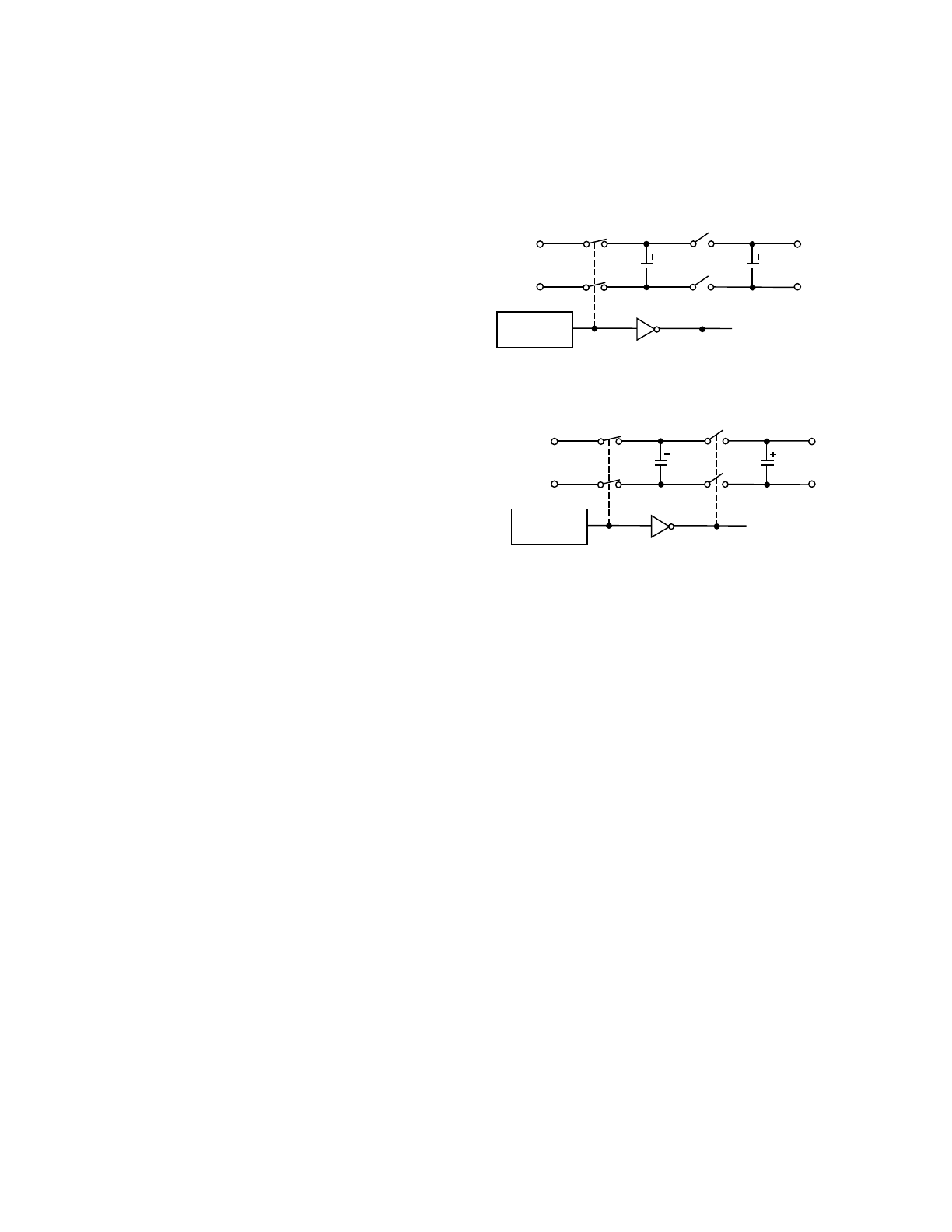
CIRCUIT DESCRIPTION
The internal circuitry consists of four main sections. These are:
1. A charge pump voltage converter
2. 5 V logic to EIA-232 transmitters
3. EIA-232 to 5 V logic receivers.
4. Transient protection circuit on all I/O lines
Charge Pump DC-DC Voltage Converter
The charge pump voltage converter consists of an 200 kHz os-
cillator and a switching matrix. The converter generates a
±
10 V
supply from the input +5 V level. This is done in two stages us-
ing a switched capacitor technique as illustrated below. First,
the 5 V input supply is doubled to 10 V using capacitor C1 as
the charge storage element. The 10 V level is then inverted to
generate –10 V using C2 as the storage element.
Capacitors C3 and C4 are used to reduce the output ripple.
Their values are not critical and can be increased if desired. On
the ADM202E, capacitor C3 is shown connected between V+
and V
CC
, while it is connected between V+ and GND on the
ADM1181A. It is acceptable to use either configuration with
both the ADM202E and ADM1181A. If desired, larger capaci-
tors (up to 47
µ
F) can be used for capacitors C1–C4. This facili-
tates direct substitution with older generation charge pump
RS-232 transceivers.
S1
S2
C1
S4
S3
C3
V+ = 2V
CC
V
CC
V
CC
GND
INTERNAL
OSCILLATOR
NOTE: C3 CONNECTS BETWEEN V+ AND GND ON THE ADM1181A
Figure 1. Charge Pump Voltage Doubler
S1
S2
C2
S4
S3
C4
V– = –(V+)
V+
GND
INTERNAL
OSCILLATOR
GND
FROM
VOLTAGE
DOUBLER
Figure 2. Charge Pump Voltage Inverter
Transmitter (Driver) Section
The drivers convert 5 V logic input levels into RS-232 output
levels. With V
CC
= +5 V and driving an RS-232 load, the output
voltage swing is typically
±
9 V.
Receiver Section
The receivers are inverting level shifters which accept RS-232
input levels and translate them into 5 V logic output levels.
The inputs have internal 5 k
Ω
pull-down resistors to ground
and are also protected against overvoltages of up to
±
30 V. Un-
connected inputs are pulled to 0 V by the internal 5 k
Ω
pull-
down resistor. This, therefore, results in a Logic 1 output level
for unconnected inputs or for inputs connected to GND.
The receivers have Schmitt trigger inputs with a hysteresis level
of 0.5 V. This ensures error-free reception for both noisy inputs
and for inputs with slow transition times.
ADM202E/ADM1181A
–5–
REV. 0
HIGH BAUD RATE
The ADM202E/ADM1181A feature high slew rates permitting
data transmission at rates well in excess of the EIA/RS-232-E
specifications. RS-232 voltage levels are maintained at data rates
up to 230 kb/s even under worst case loading conditions. This
allows for high speed data links between two terminals or indeed
it is suitable for the new generation I
SDN
modem standards which
requires data rates of 230 kbps. The slew rate is internally con-
trolled to less than 30 V/
µ
s in order to minimize EMI interference.
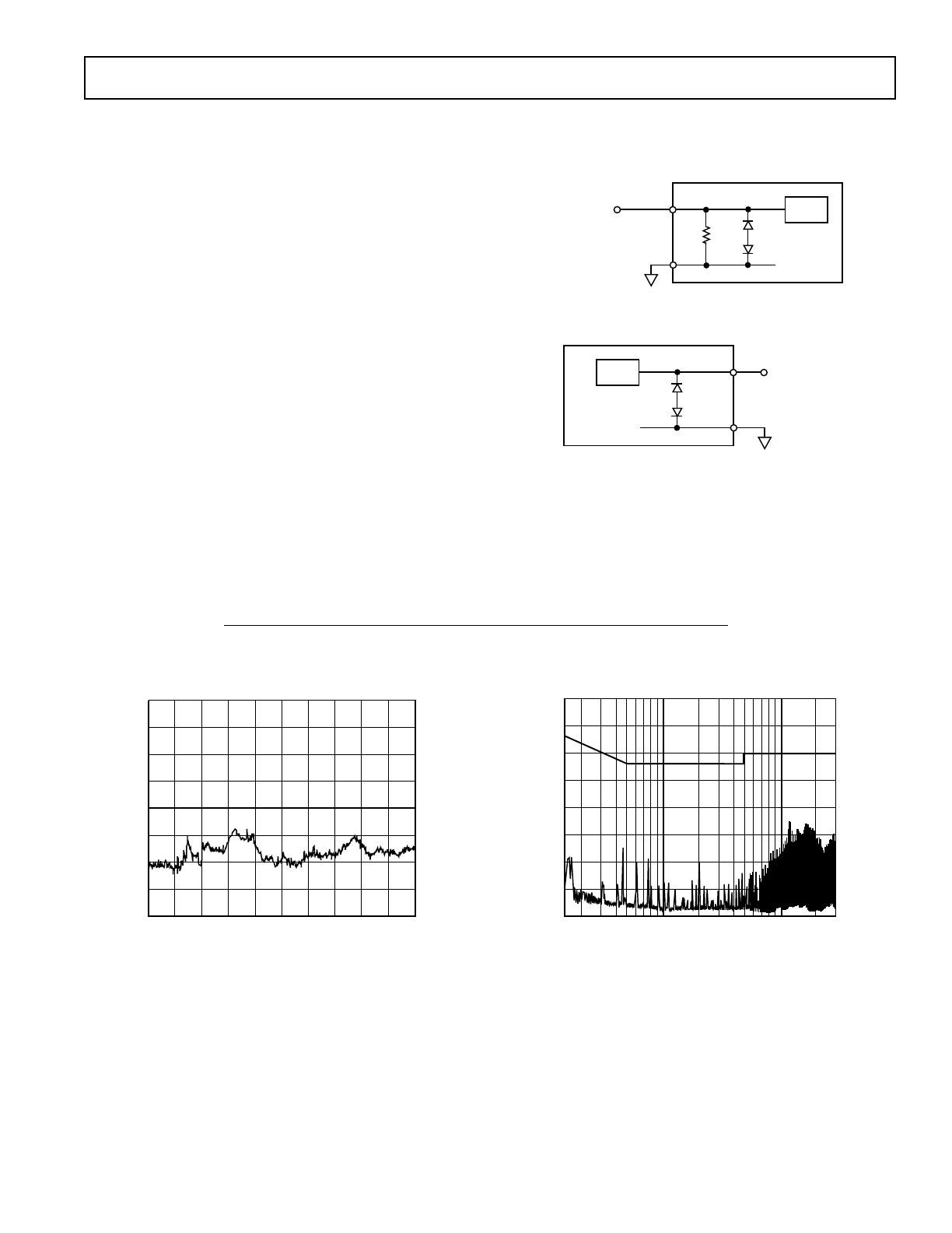
ESD/EFT TRANSIENT PROTECTION SCHEME.
The ADM202E/ADM1181A use protective clamping structures
on all inputs and outputs which clamp the voltage to a safe level
and dissipate the energy present in ESD (Electrostatic) and
EFT (Electrical Fast Transients) discharges. A simplified sche-
matic of the protection structure is shown in Figure 3. Each in-
put and output contains two back-to-back high speed clamping
diodes. During normal operation with maximum RS-232 signal
levels, the diodes have no effect as one or the other is reverse bi-
ased depending on the polarity of the signal. If however the volt-
age exceeds about 50 V in either direction, reverse breakdown
occurs and the voltage is clamped at this level. The diodes are
large p-n junctions that are designed to handle the instanta-
neous current surge which can exceed several amperes.
The transmitter outputs and receiver inputs have a similar pro-
tection structure. The receiver inputs can also dissipate some of
the energy through the internal 5 k
Ω
resistor to GND as well as
through the protection diodes.
The protection structure achieves ESD protection up to
±
15 kV
and EFT protection up to
±
2 kV on all RS-232 I/O lines. The
methods used to test the protection scheme are discussed later.
R
IN
RX
D1
D2
RECEIVER
INPUT
R1
Figure 3a. Receiver Input Protection Scheme
RX
D1
D2
TRANSMITTER
OUTPUT
T
OUT
Figure 3b. Transmitter Output Protection Scheme
Typical Performance Curves
START 30.0 MHz
STOP 200.0 MHz
LIMIT
dBµV
80
70
60
50
40
30
20
10
0
Figure 4. EMC Radiated Emissions
LOG FREQUENCY – MHz
80
70
0
0.3
30
0.6
1
60
50
10
40
30
20
3
6
10
dBµV
LIMIT
Figure 5. EMC Conducted Emissions
ADM202E/ADM1181A
–6–
REV. 0
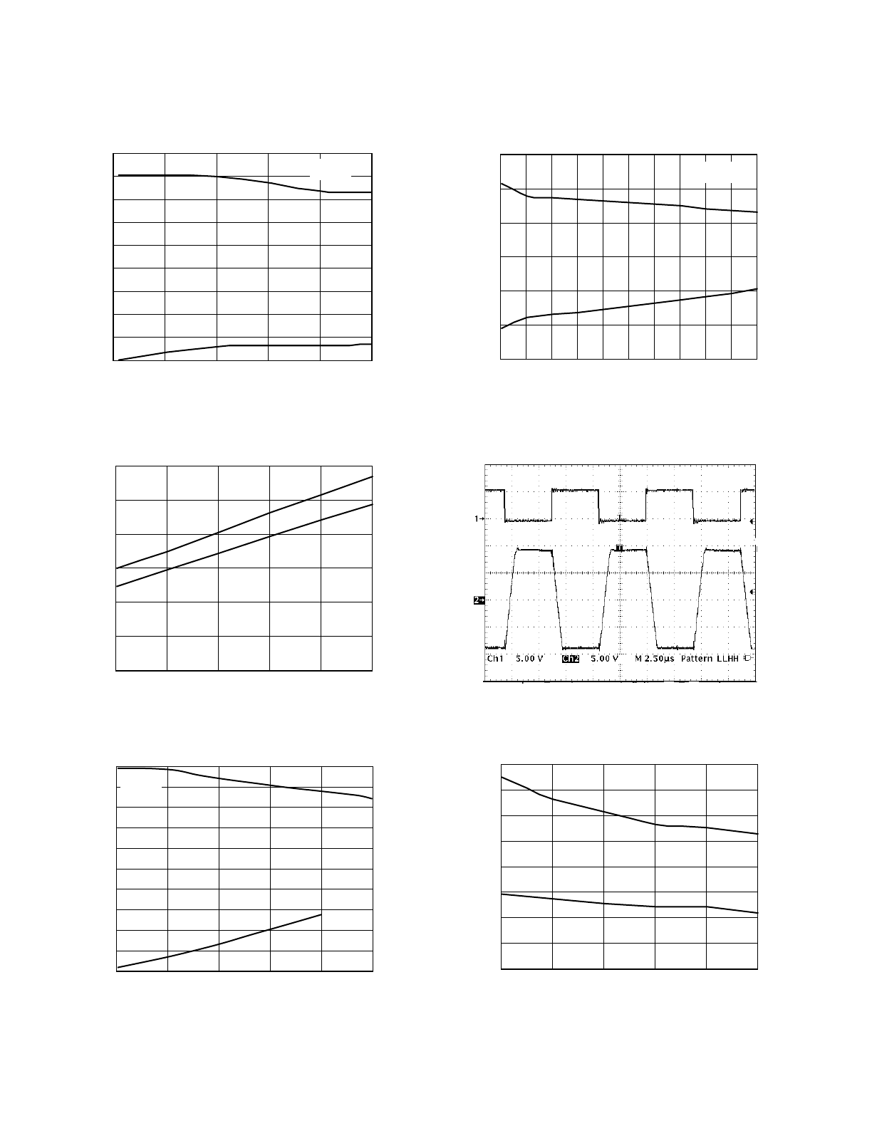
Typical Performance Curves
C
L
– pF
10
8
–8
0
2500
500
T
OUT
VOLTAGE – V
1000
1500
2000
2
–2
–4
–6
6
4
0
V
CC
= +5V
T
A
= 25
8
C
Figure 6. Transmitter Output Voltage High/Low vs.
Load Capacitance @ 230 kbps
V
CC
– V
12
10
0
3
5.5
3.5
T
OUT
– V+
4
4.5
5
8
6
4
2
T
A
= 25
8
C
Figure 7. Transmitter Output Voltage High vs. V
CC
I
LOAD
– mA
10
–10
0
5
CHARGE PUMP VOLTAGE
10
15
20
25
8
2
–2
–6
–8
6
4
0
–4
V
CC
= +5V
T
A
= 25
8
C
Figure 8. Charge Pump V+, V– vs. Current
I
LOAD
– mA
15
–15
0
10
1
T
OUT
– V
2
3
4
5
6
7
8
10
5
0
–5
–10
9
V
CC
= +5V
T
A
= 25
8
C
Figure 9. Transmitter Output Voltage Low/High vs.
Load Current
V
CC
= +5V
T
A
= 25
8
C
Figure 10. 230 kbps Data Transmission
V
CC
– V
400
350
0
3
5.5
3.5
IMPEDANCE –
Ω
4
4.5
5
200
150
100
50
300
250
T
A
= 25
8
C
Figure 11. Charge Pump Impedance vs. V
CC
ADM202E/ADM1181A
–7–
REV. 0
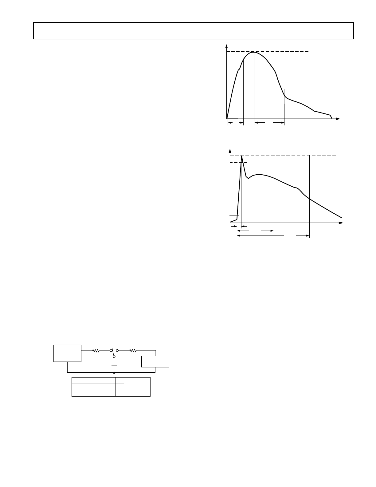
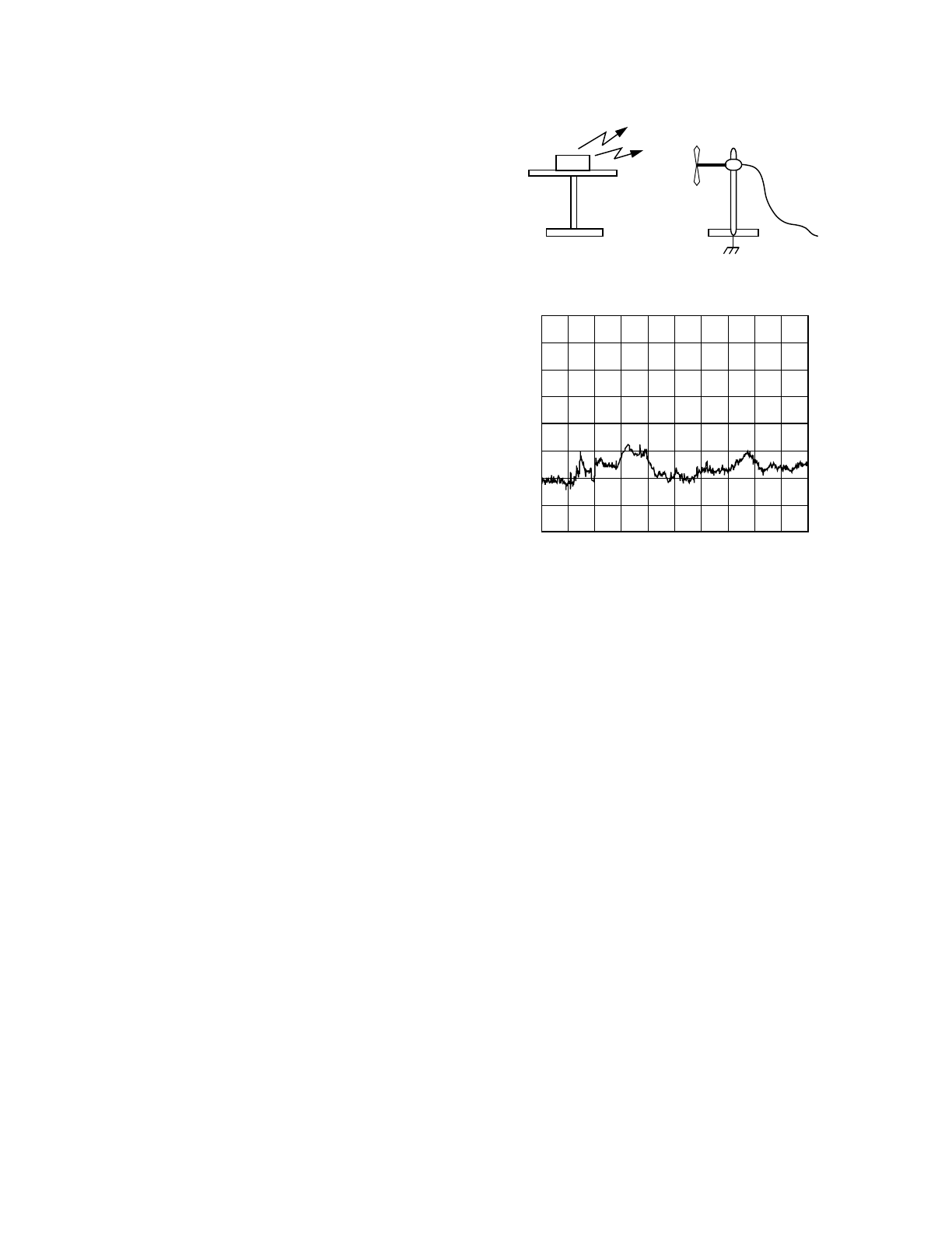
ESD TESTING (IEC1000-4-2)
IEC1000-4-2 (previously 801-2) specifies compliance testing
using two coupling methods, contact discharge and air-gap
discharge. Contact discharge calls for a direct connection to the
unit being tested. Air-gap discharge uses a higher test voltage
but does not make direct contact with the unit under test. With
air discharge, the discharge gun is moved towards the unit un-
der test developing an arc across the air gap, hence the term air-
gap discharge. This method is influenced by humidity, tempera-
ture, barometric pressure, distance and rate of closure of the dis-
charge gun. The contact-discharge method while less realistic is
more repeatable and is gaining acceptance in preference to the
air-gap method.
Although very little energy is contained within an ESD pulse,
the extremely fast rise time coupled with high voltages can cause
failures in unprotected semiconductors. Catastrophic destruc-
tion can occur immediately as a result of arcing or heating. Even
if catastrophic failure does not occur immediately, the device
may suffer from parametric degradation which may result in de-
graded performance. The cumulative effects of continuous ex-
posure can eventually lead to complete failure.
I/O lines are particularly vulnerable to ESD damage. Simply
touching or plugging in an I/O cable can result in a static dis-
charge which can damage or completely destroy the interface
product connected to the I/O port. Traditional ESD test meth-
ods such as the MIL-STD-883B method 3015.7 do not fully
test a product’s susceptibility to this type of discharge. This test
was intended to test a product’s susceptibility to ESD damage
during handling. Each pin is tested with respect to all other
pins. There are some important differences between the tradi-
tional test and the IEC test:
a. The IEC test is much more stringent in terms of discharge
energy. The peak current injected is over four times greater.
b. The current rise time is significantly faster in the IEC test.
c. The IEC test is carried out while power is applied to the device.
It is possible that the ESD discharge could induce latch-up in
the device under test. This test therefore is more representative
of a real-world I/O discharge where the equipment is operating
normally with power applied. For maximum peace of mind,
however, both tests should be performed therefore ensuring
maximum protection both during handling and later during field
service.
R1
R2
C1
DEVICE
UNDER TEST
HIGH
VOLTAGE
GENERATOR
ESD TEST METHOD
R2
C1
H. BODY MIL-STD883B
1.5k
Ω
100pF
IEC1000-4-2
330
Ω
150pF
Figure 12. ESD Test Standards
100
I
PEAK
– %
90
36.8
10
t
DL
t
RL
TIME t
Figure 13. Human Body Model ESD Current Waveform
100
I
PEAK
– %
90
10
TIME t
30ns
60ns
0.1 TO 1ns
Figure 14. IEC1000-4-2 ESD Current Waveform
The ADM202E/ADM1181E products are tested using both the
above mentioned test methods. All pins are tested with respect
to all other pins as per the MIL-STD-883B specification. In ad-
dition all I/O pins are tested as per the IEC test specification.
The products were tested under the following conditions:
a. Power-On
b. Power-Off
There are four levels of compliance defined by IEC1000-4-2.
The ADM202E/ADM1181A products meet the most stringent
compliance level for both contact and for air-gap discharge.
This means that the products are able to withstand contact dis-
charges in excess of 8 kV and air-gap discharges in excess of
15 kV.
ADM202E/ADM1181A
–8–
REV. 0
Table I. IEC1000-4-2 Compliance Levels
Level
Contact Discharge
Air Discharge
1
2 kV
2 kV
2
4 kV
4 kV
3
6 kV
8 kV
4
8 kV
15 kV
Table II. ADM202E/ADM1181A ESD Test Results
ESD Test Method
I/O Pins
Other Pins
MIL-STD-883B
±
15 kV
±
3 kV
IEC1000-4-2
Contact
±
8 kV
Air
±
15 kV
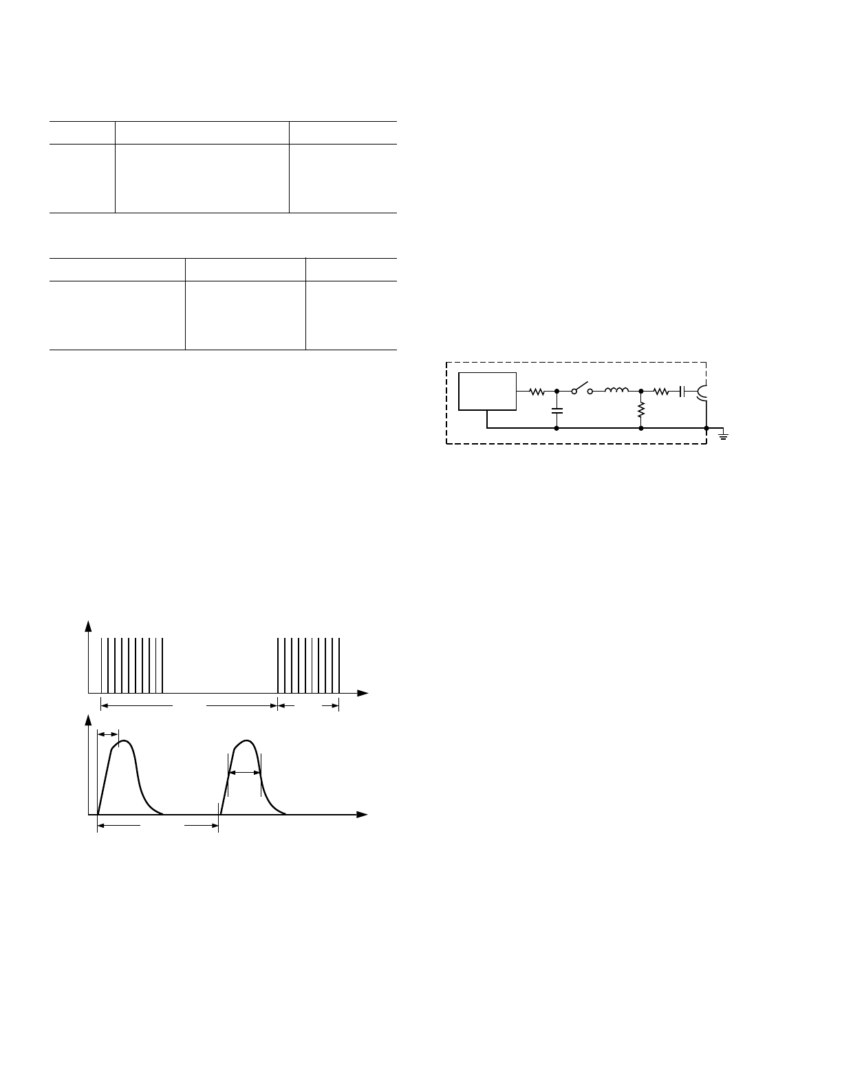
FAST TRANSIENT BURST TESTING (IEC1000-4-4)
IEC1000-4-4 (previously 801-4) covers electrical fast-transient/
burst (EFT) immunity. Electrical fast transients occur as a re-
sult of arcing contacts in switches and relays. The tests simulate
the interference generated when for example a power relay dis-
connects an inductive load. A spark is generated due to the well
known back EMF effect. In fact the spark consists of a burst of
sparks as the relay contacts separate. The voltage appearing on
the line therefore consists of a bust of extremely fast transient
impulses. A similar effect occurs when switching on fluorescent
lights.
The fast transient burst test defined in IEC1000-4-4 simulates
this arcing and its waveform is illustrated in Figure 11. It con-
sists of a burst of 2.5 kHz to 5 kHz transients repeating at
300 ms intervals. It is specified for both power and data lines.
300ms
15ms
t
V
5ns
0.2/0.4ms
50ns
V
t
Figure 15. IEC1000-4-4 Fast Transient Waveform
A simplified circuit diagram of the actual EFT generator is illus-
trated in Figure 16.
The transients are coupled onto the signal lines using an EFT
coupling clamp. The clamp is 1 m long and it completely sur-
rounds the cable providing maximum coupling capacitance
(50 pF to 200 pF typ) between the clamp and the cable. High
energy transients are capacitively coupled onto the signal lines.
Fast rise times (5 ns) as specified by the standard result in very
effective coupling. This test is very severe since high voltages are
coupled onto the signal lines. The repetitive transients can often
cause problems where single pulses don’t. Destructive latchup
may be induced due to the high energy content of the tran-
sients. Note that this stress is applied while the interface prod-
ucts are powered up and are transmitting data. The EFT test
applies hundreds of pulses with higher energy than ESD. Worst
case transient current on an I/O line can be as high as 40 A.
R
C
R
M
C
C
HIGH
VOLTAGE
SOURCE
L
Z
S
C
D
50
Ω
OUTPUT
Figure 16. IEC1000-4-4 Fast Transient Generator
Test results are classified according to the following:
1. Normal performance within specification limits.
2. Temporary degradation or loss of performance that is
self-recoverable.
3. Temporary degradation or loss of function or performance
that requires operator intervention or system reset.
4. Degradation or loss of function that is not recoverable due
to damage.
The ADM202E/ADM1181A have been tested under worst case
conditions using unshielded cables and meet Classification 2.
Data transmission during the transient condition is corrupted,
but it may be resumed immediately following the EFT event
without user intervention.
ADM202E/ADM1181A
–9–
REV. 0
IEC1000-4-3 RADIATED IMMUNITY
IEC1000-4-3 (previously IEC801-3) describes the measurement
method and defines the levels of immunity to radiated electro-
magnetic fields. It was originally intended to simulate the elec-
tromagnetic fields generated by portable radio transceivers or
any other device which generates continuous wave radiated
electromagnetic energy. Its scope has since been broadened to
include spurious EM energy which can be radiated from fluores-
cent lights, thyristor drives, inductive loads, etc.
Testing for immunity involves irradiating the device with an EM
field. There are various methods of achieving this including use
of anechoic chamber, stripline cell, TEM cell, GTEM cell. A
stripline cell consists of two parallel plates with an electric field
developed between them. The device under test is placed within
the cell and exposed to the electric field. There are three severity
levels having field strengths ranging from 1 V to 10 V/m. Results
are classified in a similar fashion to those for IEC1000-4-2.
1. Normal Operation.
2. Temporary Degradation or loss of function that is self-
recoverable when the interfering signal is removed.
3. Temporary degradation or loss of function that requires
operator intervention or system reset when the interfering
signal is removed.
4. Degradation or loss of function that is not recoverable due to
damage.
The ADM202E/ADM1181A products easily meet Classification
1 at the most stringent (Level 3) requirement. In fact field
strengths up to 30 V/m showed no performance degradation,
and error-free data transmission continued even during irradia-
tion.
Table III. Test Severity Levels (IEC1000-4-3)
Level
Field Strength V/m
1
1
2
3
3
10
EMISSIONS/INTERFERENCE
EN55 022, CISPR22 defines the permitted limits of radiated
and conducted interference from Information Technology (IT)
equipment. The objective of the standard is to minimize the
level of emissions both conducted and radiated.
For ease of measurement and analysis, conducted emissions are
assumed to predominate below 30 MHz and radiated emissions
are assumed to predominate above 30 MHz.
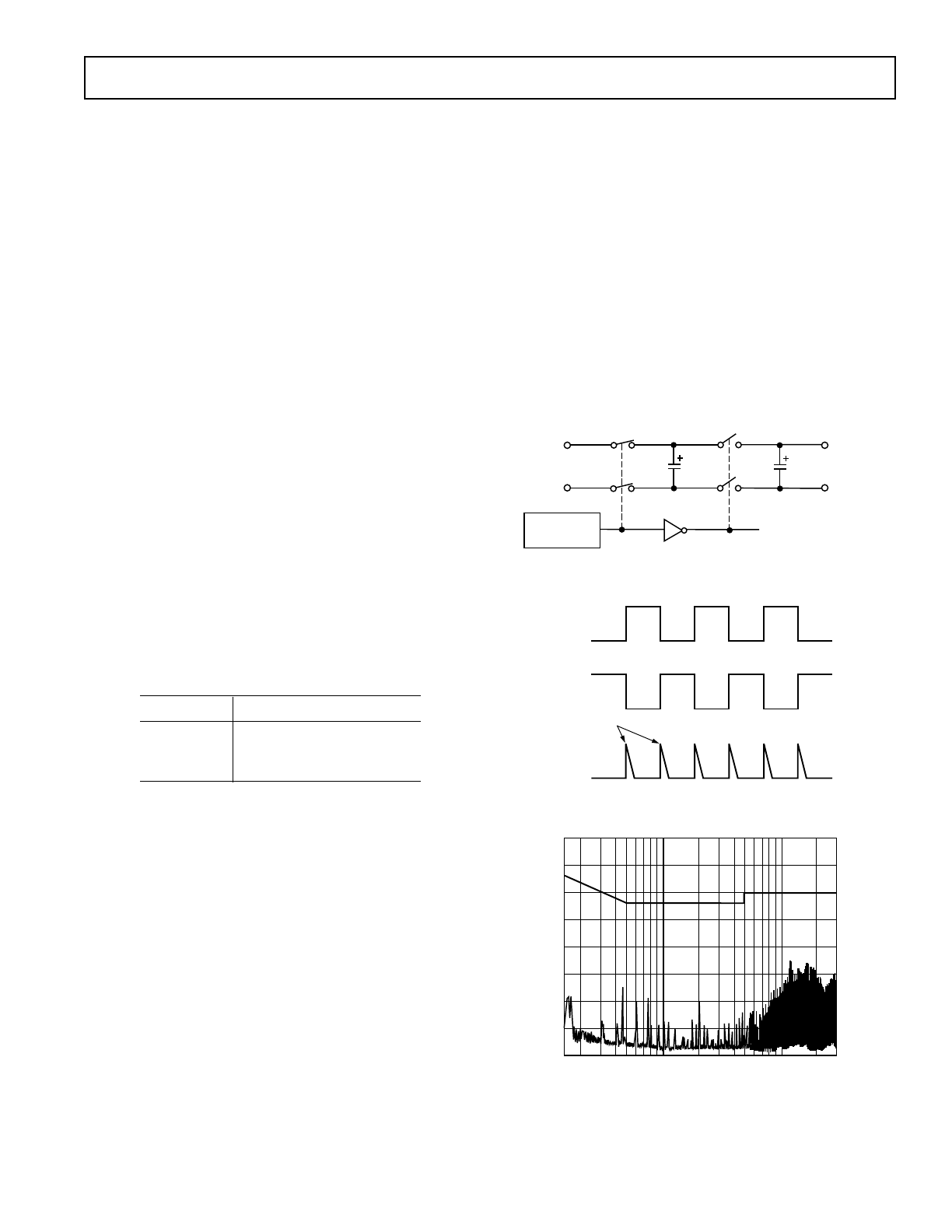
CONDUCTED EMISSIONS
This is a measure of noise that gets conducted onto the mains
power supply. Switching transients from the charge pump that
are 20 V in magnitude and contain significant energy can lead to
conducted emissions. Other sources of conducted emissions can
be due to overlap in switch on-times in the charge pump voltage
converter. In the voltage doubler shown below, if S2 has not
fully turned off before S4 turns on, this results in a transient
current glitch between V
CC
and GND which results in con-
ducted emissions. It is, therefore, important that the switches in
the charge pump guarantee break-before-make switching under
all conditions so that instantaneous short circuit conditions do
not occur.
The ADM202E has been designed to minimize the switching
transients and ensure break-before-make switching thereby
minimizing conducted emissions. This has resulted in the level
of emissions being well below the limits required by the specifi-
cation. No additional filtering/decoupling other than the recom-
mended 0.1
µ
F capacitor is required.
Conducted emissions are measured by monitoring the mains
line. The equipment used consists of a LISN (Line Impedance
Stabilizing Network) that essentially presents a fixed impedance
at RF, and a spectrum analyzer. The spectrum analyzer scans
for emissions up to 30 MHz and a plot for the ADM202E is
shown in Figure 19.
S1
S2
C1
S4
S3
C3
V+ = 2V
C C
V
CC
INTERNAL
OSCILLATOR
GND
V
CC
Figure 17. Charge Pump Voltage Doubler
ø
1
ø
2
SWITCHING GLITCHES
Figure 18. Switching Glitches
LOG FREQUENCY – MHz
80
70
0
0.3
30
0.6
1
60
50
10
40
30
20
3
6
10
dBµV
LIMIT
Figure 19. ADM202E Conducted Emissions Plot
ADM202E/ADM1181A
–10–
REV. 0
RADIATED EMISSIONS
Radiated emissions are measured at frequencies in excess of
30 MHz. RS-232 outputs designed for operation at high baud
rates while driving cables can radiate high frequency EM energy.
The reasons already discussed that cause conducted emissions
can also be responsible for radiated emissions. Fast RS-232 out-
put transitions can radiate interference, especially when lightly
loaded and driving unshielded cables. Charge pump devices are
also prone to radiating noise due to the high frequency oscillator
and high voltages being switched by the charge pump. The
move towards smaller capacitors in order to conserve board
space has resulted in higher frequency oscillators being em-
ployed in the charge pump design. This has resulted in higher
levels of emission, both conducted and radiated.
The RS-232 outputs on the ADM202E products feature a con-
trolled slew rate in order to minimize the level of radiated emis-
sions, yet are fast enough to support data rates up to 230 kBaud.
Figure 21 shows a plot of radiated emissions vs. frequency. This
shows that the levels of emissions are well within specifications
without the need for any additional shielding or filtering compo-
nents. The ADM202E was operated at maximum baud rates
and configured as in a typical RS-232 interface.
Testing for radiated emissions was carried out in a shielded
anechonic chamber.
TURNTABLE
DUT
RADIATED NOISE
ADJUSTABLE
ANTENNA
TO
RECEIVER
Figure 20. Radiated Emissions Test Setup
START 30.0 MHz
STOP 200.0 MHz
LIMIT
dBµV
80
70
60
50
40
30
20
10
0
Figure 21. ADM202E Radiated Emissions Plot
ADM202E/ADM1181A
–11–
REV. 0
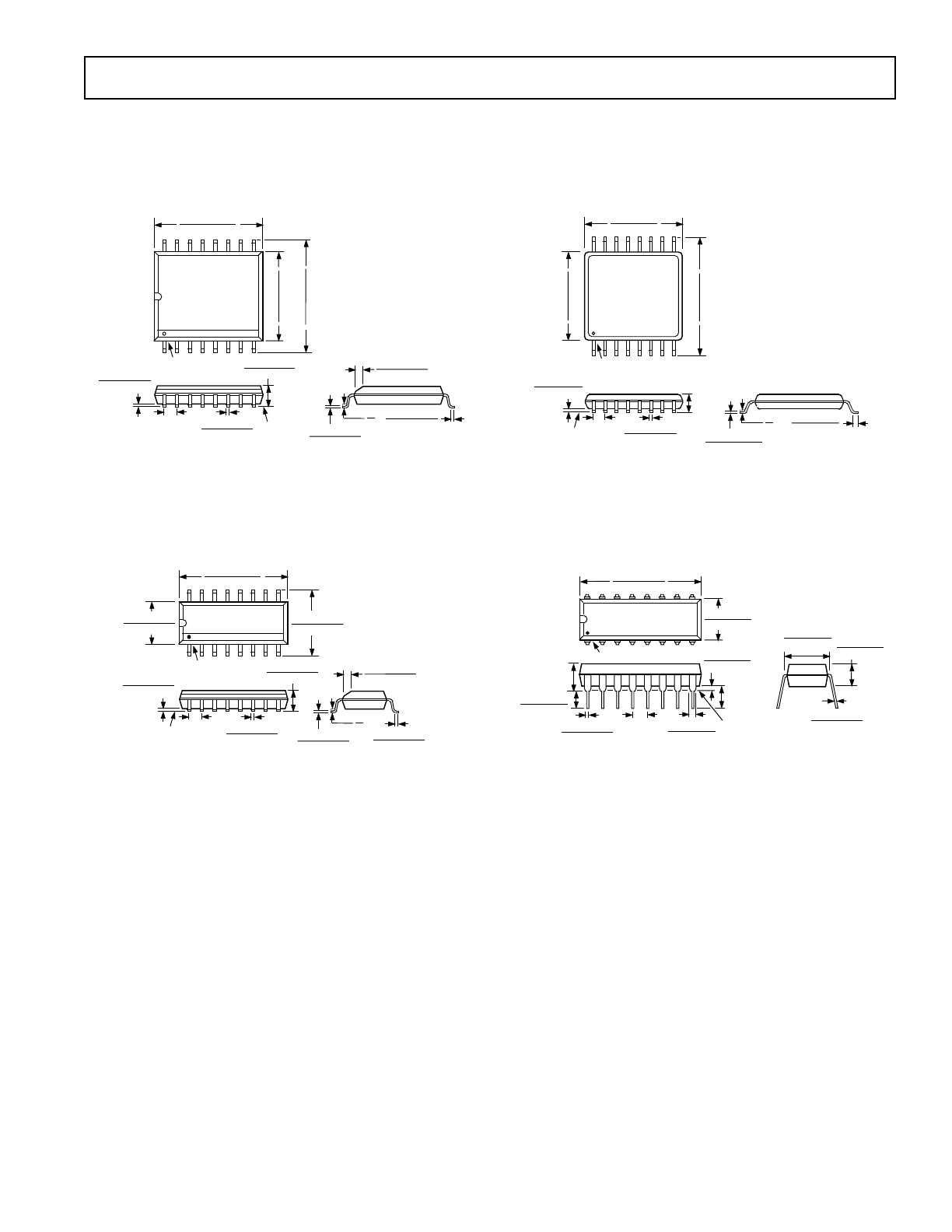
OUTLINE DIMENSIONS
Dimensions shown in inches and (mm).
TSSOP Package
(RU-16)
16
9
8
1
0.201 (5.10)
0.193 (4.90)
0.256 (6.50)
0.246 (6.25)
0.177 (4.50)
0.169 (4.30)
PIN 1
SEATING
PLANE
0.006 (0.15)
0.002 (0.05)
0.0118 (0.30)
0.0075 (0.19)
0.0256
(0.65)
BSC
0.0433
(1.10)
MAX
0.0079 (0.20)
0.0035 (0.090)
0.028 (0.70)
0.020 (0.50)
8
°
0
°
DIP Package
(N-16)
16
1
8
9
0.840 (21.33)
0.745 (18.93)
0.280 (7.11)
0.240 (6.10)
PIN 1
SEATING
PLANE
0.022 (0.558)
0.014 (0.356)
0.060 (1.52)
0.015 (0.38)
0.210 (5.33)
MAX
0.130
(3.30)
MIN
0.070 (1.77)
0.045 (1.15)
0.100
(2.54)
BSC
0.160 (4.06)
0.115 (2.93)
0.325 (8.25)
0.300 (7.62)
0.015 (0.381)
0.008 (0.204)
0.195 (4.95)
0.115 (2.93)
SOIC (Wide) Package
(R-16W)
16
9
8
1
0.4133 (10.50)
0.3977 (10.00)
0.4193 (10.65)
0.3937 (10.00)
0.2992 (7.60)
0.2914 (7.40)
PIN 1
SEATING
PLANE
0.0118 (0.30)
0.0040 (0.10)
0.0192 (0.49)
0.0138 (0.35)
0.1043 (2.65)
0.0926 (2.35)
0.0500
(1.27)
BSC
0.0125 (0.32)
0.0091 (0.23)
0.0500 (1.27)
0.0157 (0.40)
8
°
0
°
0.0291 (0.74)
0.0098 (0.25)
x 45
°
SOIC (Narrow) Package
(R-16N)
16
9
8
1
0.3937 (10.00)
0.3859 (9.80)
0.2440 (6.20)
0.2284 (5.80)
0.1574 (4.00)
0.1497 (3.80)
PIN 1
SEATING
PLANE
0.0098 (0.25)
0.0040 (0.10)
0.0192 (0.49)
0.0138 (0.35)
0.0688 (1.75)
0.0532 (1.35)
0.0500
(1.27)
BSC
0.0099 (0.25)
0.0075 (0.19)
0.0500 (1.27)
0.0160 (0.41)
8
°
0
°
0.0196 (0.50)
0.0099 (0.25)
x 45
°

C2162–18–7/96
PRINTED IN U.S.A.
–12–