
FUNCTIONAL BLOCK DIAGRAM
D2
S1
S2
S3
S4
D1
D3
D4
IN1
IN2
IN3
IN4
ADG511
SWITCHES SHOWN FOR A LOGIC “1” INPUT
S2
D2
D3
S1
S3
S4
D1
D4
IN1
IN2
IN3
IN4
ADG512
D2
S1
S2
S3
S4
D1
D3
D4
IN1
IN2
IN3
IN4
ADG513
REV. 0
Information furnished by Analog Devices is believed to be accurate and
reliable. However, no responsibility is assumed by Analog Devices for its
use, nor for any infringements of patents or other rights of third parties
which may result from its use. No license is granted by implication or
otherwise under any patent or patent rights of Analog Devices.
a
DI LC
2
MOS
Precision 5 V/3 V Quad SPST Switches
ADG511/ADG512/ADG513
One Technology Way, P.O. Box 9106, Norwood, MA 02062-9106, U.S.A.
Tel: 617/329-4700
Fax: 617/326-8703
FEATURES
+3 V, +5 V or
65 V Power Supplies
Ultralow Power Dissipation (<0.5
mW)
Low Leakage (<100 pA)
Low On Resistance (<50
V)
Fast Switching Times
Low Charge Injection
Latch-Up Proof
TTL/CMOS Compatible
16-Pin DIP or SOIC Package
APPLICATIONS
Battery Powered Instruments
Single Supply Systems
Remote Powered Equipment
+5 V Supply Systems
Computer Peripherals such as Disk Drives
Precision Instrumentation
Audio and Video Switching
Automatic Test Equipment
Precision Data Acquisition
Sample Hold Systems
Communication Systems
Compatible with
65 V Supply DACs and ADCs such as
AD7840/8, AD7870/1/2/4/5/6/8
GENERAL DESCRIPTION
The ADG511, ADG512 and ADG513 are monolithic CMOS
ICs containing four independently selectable analog switches.
These switches feature low, well-controlled on resistance and
wide analog signal range, making them ideal for precision
analog signal switching.
These switch arrays are fabricated using Analog Devices’
advanced linear compatible CMOS (LC
2
MOS) process which
offers the additional benefits of low leakage currents, ultralow
power dissipation and low capacitance for fast switching speeds
with minimum charge injection. These features make the
ADG511, ADG512 and ADG513 the optimum choice for a
wide variety of signal switching tasks in precision analog signal
processing and data acquisition systems.
The ability to operate from single +3 V, +5 V or
±
5 V bipolar
supplies make the ADG511, ADG512 and ADG513 perfect for
use in battery-operated instruments, 4–20 mA loop systems and
with the new generation of DACs and ADCs from Analog
Devices. The use of 5 V supplies and reduced operating currents
give much lower power dissipation than devices operating from
±
15 V supplies.
The ADG511, ADG512 and ADG513 contain four indepen-
dent SPST switches. The ADG511 and ADG512 differ only in
that the digital control logic is inverted. The ADG511 switch is
turned on with a logic low on the appropriate control input,
while a logic high is required for the ADG512. The ADG513
contains two switches whose digital control logic is similar to
that of the ADG511 while the logic is inverted in the remaining
two switches.
PRODUCT HIGHLIGHTS
1. +5 Volt Single Supply Operation
The ADG511/ADG512/ADG513 offers high performance,
including low on resistance and wide signal range, fully
specified and guaranteed with +3 V,
±
5 V as well as +5 V
supply rails.
2. Ultralow Power Dissipation
CMOS construction ensures ultralow power dissipation.
3. Low R
ON
4. Trench Isolation Guards Against Latch-up
A dielectric trench separates the P and N channel transistors
thereby preventing latch-up even under severe overvoltage
conditions.
5. Break Before Make Switching
Switches are guaranteed to have break-before-make opera-
tion. This allows multiple outputs to be tied together for
multiplexer applications without the possibility of momentary
shorting between channels.

ADG511/ADG512/ADG513–SPECIFICATIONS
1
Dual Supply
B Version
T Version
–40
8C to
–55
8C to
Parameter
+25
8C
+85
8C
+25
8C
+125
8C
Units
Test Conditions/Comments
ANALOG SWITCH
Analog Signal Range
V
DD
to V
SS
V
DD
to V
SS
V
R
ON
30
30
Ω
typ
V
D
=
±
3.5 V, I
S
= –10 mA;
50
50
Ω
max
V
DD
= +4.5 V, V
SS
= –4.5 V
LEAKAGE CURRENTS
V
DD
= +5.5 V, V
SS
= –5.5 V
Source OFF Leakage I
S
(OFF)
±
0.025
±
0.025
nA typ
V
D
=
±
4.5 V, V
S
=
74.5 V;
±
0.1
±
2.5
±
0.1
±
2.5
nA max
Test Circuit 2
Drain OFF Leakage I
D
(OFF)
±
0.025
±
0.025
nA typ
V
D
=
±
4.5 V, V
S
=
74.5 V;
±
0.1
±
2.5
±
0.1
±
2.5
nA max
Test Circuit 2
Channel ON Leakage I
D
, I
S
(ON)
±
0.05
±
0.05
nA typ
V
D
= V
S
=
±
4.5 V;
±
0.2
±
5
±
0.2
±
5
nA max
Test Circuit 3
DIGITAL INPUTS
Input High Voltage, V
INH
2.4
2.4
V min
Input Low Voltage, V
INL
0.8
0.8
V max
Input Current
I
INL
or I
INH
0.005
0.005
µ
A typ
V
IN
= V
INL
or V
INH
±
0.1
±
0.1
µ
A max
DYNAMIC CHARACTERISTICS
2
t
ON
200
200
ns typ
R
L
= 300
Ω
. C
L
= 35 pF;
375
375
ns max
V
S
=
±
3 V; Test Circuit 4
t
OFF
120
120
ns typ
R
L
= 300
Ω
. C
L
= 35 pF;
150
150
ns max
V
S
=
±
3 V; Test Circuit 4
Break-Before-Make Time
100
100
ns typ
R
L
= 300
Ω
, C
L
= 35 pF;
Delay, t
D
(ADG513 Only)
V
S1
= V
S2
= +3 V; Test Circuit 5
Charge Injection
11
11
pC typ
V
S
= 0 V, R
S
= 0
Ω
, C
L
= 10 nF;
Test Circuit 6
OFF Isolation
68
68
dB typ
R
L
= 50
Ω
, C
L
= 5 pF, f = 1 MHz;
Test Circuit 7
Channel-to-Channel Crosstalk
85
85
dB typ
R
L
= 50
Ω
, C
L
= 5 pF, f = 1 MHz;
Test Circuit 8
C
S
(OFF)
9
9
pF typ
f = 1 MHz
C
D
(OFF)
9
9
pF typ
f = 1 MHz
C
D
, C
S
(ON)
35
35
pF typ
f = 1 MHz
POWER REQUIREMENTS
V
DD
+4.5/5.5
+4.5/5.5
V min/max
V
SS
–4.5/–5.5
–4.5/–5.5
V min/max
I
DD
0.0001
0.0001
µ
A typ
V
DD
= +5.5 V, V
SS
= –5.5 V
1
1
µ
A max
Digital Inputs = 0 V or 5 V
I
SS
0.0001
0.0001
µ
A typ
1
1
µ
A max
NOTES
1
Temperature ranges are as follows: B Versions –40
°
C to +85
°
C; T Versions –55
°
C to +125
°
C.
2
Guaranteed by design, not subject to production test.
Specifications subject to change without notice.
REV. 0
–2–
(V
DD
= +5 V
6 10%, V
SS
= –5 V
6 10%, GND = 0 V, unless otherwise noted)

Single Supply
B Version
T Version
–40
8C to
–55
8C to
Parameter
+25
8C
+85
8C
+25
8C
+125
8C
Units
Test Conditions/Comments
ANALOG SWITCH
Analog Signal Range
0 V to V
DD
0 V to V
DD
V
R
ON
45
45
Ω
typ
V
D
= +3.5 V, I
S
= –10 mA;
75
75
Ω
max
V
DD
= +4.5 V
LEAKAGE CURRENTS
V
DD
= +5.5 V
Source OFF Leakage I
S
(OFF)
±
0.025
±
0.025
nA typ
V
D
= 4.5/1 V, V
S
= 1
/4.5 V;
±
0.1
±
2.5
±
0.1
±
2.5
nA max
Test Circuit 2
Drain OFF Leakage I
D
(OFF)
±
0.025
±
0.025
nA typ
V
D
= 4.5/1 V, V
S
= 1
/4.5 V;
±
0.1
±
2.5
±
0.1
±
2.5
nA max
Test Circuit 2
Channel ON Leakage I
D
, I
S
(ON)
±
0.05
±
0.05
nA typ
V
D
= V
S
= +4.5 V/+1 V;
±
0.2
±
5
±
0.2
±
5
nA max
Test Circuit 3
DIGITAL INPUTS
Input High Voltage, V
INH
2.4
2.4
V min
Input Low Voltage, V
INL
0.8
0.8
V max
Input Current
I
INL
or I
INH
0.005
0.005
µ
A typ
V
IN
= V
INL
or V
INH
±
0.1
±
0.1
µ
A max
DYNAMIC CHARACTERISTICS
2
t
ON
250
250
ns typ
R
L
= 300
Ω
, C
L
= 35 pF;
500
500
ns max
V
S
= +2 V; Test Circuit 4
t
OFF
50
50
ns typ
R
L
= 300
Ω
, C
L
= 35 pF;
100
100
ns max
V
S
= +2 V; Test Circuit 4
Break-Before-Make Time
200
200
ns typ
R
L
= 300
Ω
, C
L
= 35 pF;
Delay, t
D
(ADG513 Only)
V
S1
= V
S2
= +2 V; Test Circuit 5
Charge Injection
16
16
pC typ
V
S
= 0 V, R
S
= 0
Ω
, C
L
= 10 nF;
Test Circuit 6
OFF Isolation
68
68
dB typ
R
L
= 50
Ω
, C
L
= 5 pF, f = 1 MHz;
Test Circuit 7
Channel-to-Channel Crosstalk
85
85
dB typ
R
L
= 50
Ω
, C
L
= 5 pF, f = 1 MHz;
Test Circuit 8
C
S
(OFF)
9
9
pF typ
f = 1 MHz
C
D
(OFF)
9
9
pF typ
f = 1 MHz
C
D
, C
S
(ON)
35
35
pF typ
f = 1 MHz
POWER REQUIREMENTS
V
DD
+4.5/5.5
+4.5/5.5
V min/max
I
DD
0.0001
0.0001
µ
A typ
V
DD
= +5.5 V
1
1
µ
A max
Digital Inputs = 0 V or 5 V
NOTES
1
Temperature ranges are as follows: B Versions –40
°
C to +85
°
C; T Versions –55
°
C to +125
°
C.
2
Guaranteed by design, not subject to production test.
Specifications subject to change without notice.
(V
DD
= +5 V
6 10%, V
SS
= 0 V, GND = 0 V, unless otherwise noted)
ADG511/ADG512/ADG513
REV. 0
–3–

Single Supply
B Version
0
8C to
Parameter
+25
8C
+70
8C
Units
Test Conditions/Comments
ANALOG SWITCH
Analog Signal Range
0 V to V
DD
V
R
ON
200
Ω
typ
V
D
= +1.5 V, I
S
= –1 mA;
500
Ω
max
V
DD
= +3 V,
LEAKAGE CURRENTS
V
DD
= +3.6 V
Source OFF Leakage I
S
(OFF)
±
0.025
nA typ
V
D
= 2.6/1 V, V
S
= 1
/2.6 V;
±
0.1
±
2.5
nA max
Test Circuit 2
Drain OFF Leakage I
D
(OFF)
±
0.025
nA typ
V
D
= 2.6/1 V, V
S
= 1
/2.6 V;
±
0.1
±
2.5
nA max
Test Circuit 2
Channel ON Leakage I
D
, I
S
(ON)
±
0.05
nA typ
V
D
= V
S
= +2.6 V/+1 V;
±
0.2
±
5
nA max
Test Circuit 3
DIGITAL INPUTS
Input High Voltage, V
INH
2.4
V min
Input Low Voltage, V
INL
0.8
V max
Input Current
I
INL
or I
INH
0.005
µ
A typ
V
IN
= V
INL
or V
INH
±
0.1
µ
A max
DYNAMIC CHARACTERISTICS
2
t
ON
600
ns typ
R
L
= 300
Ω
, C
L
= 35 pF;
1200
ns max
V
S
= +1 V; Test Circuit 4
t
OFF
100
ns typ
R
L
= 300
Ω
, C
L
= 35 pF;
160
ns max
V
S
= +1 V; Test Circuit 4
Break-Before-Make Time
500
ns typ
R
L
= 300
Ω
, C
L
= 35 pF;
Delay, t
D
(ADG513 Only)
V
S1
= V
S2
= +1 V; Test Circuit 5
Charge Injection
11
pC typ
V
S
= 0 V, R
S
= 0
Ω
, C
L
= 10 nF;
Test Circuit 6
OFF Isolation
68
dB typ
R
L
= 50
Ω
, C
L
= 5 pF, f = 1 MHz;
Test Circuit 7
Channel-to-Channel Crosstalk
85
dB typ
R
L
= 50
Ω
, C
L
= 5 pF, f = 1 MHz;
Test Circuit 8
C
S
(OFF)
9
pF typ
f = 1 MHz
C
D
(OFF)
9
pF typ
f = 1 MHz
C
D
, C
S
(ON)
35
pF typ
f = 1 MHz
POWER REQUIREMENTS
V
DD
3/3.6
V min/max
I
DD
0.0001
µ
A typ
V
DD
= +3.6 V
1
µ
A max
Digital Inputs = 0 V or 3 V
NOTES
1
Temperature ranges are as follows: B Versions –40
°
C to +70
°
C.
2
Guaranteed by design, not subject to production test.
REV. 0
–4–
ADG511/ADG512/ADG513–SPECIFICATIONS
1
(V
DD
= +3.3 V
6 10%, V
SS
= 0 V, GND = 0 V, unless otherwise noted)
ADG511/ADG512/ADG513
REV. 0
–5–
ABSOLUTE MAXIMUM RATINGS*
(T
A
= +25
°
C unless otherwise noted)
V
DD
to V
SS
. . . . . . . . . . . . . . . . . . . . . . . . . . . . . . . . . . . +44 V
V
DD
to GND . . . . . . . . . . . . . . . . . . . . . . . . . . –0.3 V to +25 V
V
SS
to GND . . . . . . . . . . . . . . . . . . . . . . . . . . . +0.3 V to –25 V
Analog, Digital Inputs
1
. . . . . . . . . . . V
SS
–2 V to V
DD
+ 2 V or
30 mA, Whichever Occurs First
Continuous Current, S or D . . . . . . . . . . . . . . . . . . . . . . 30 mA
Peak Current, S or D . . . . . . . . . . . . . . . . . . . . . . . . . . . 100 mA
(Pulsed at 1 ms, 10% Duty Cycle max)
Operating Temperature Range
Industrial (B Version) . . . . . . . . . . . . . . . . . . –40
°
C to +85
°
C
Extended (T Version) . . . . . . . . . . . . . . . . . –55
°
C to +125
°
C
Storage Temperature Range . . . . . . . . . . . . . –65
°
C to +150
°
C
Junction Temperature . . . . . . . . . . . . . . . . . . . . . . . . . . +150
°
C
Cerdip Package, Power Dissipation . . . . . . . . . . . . . . . 900 mW
θ
JA
Thermal Impedance . . . . . . . . . . . . . . . . . . . . . . . 76
°
C/W
Lead Temperature, Soldering (10 sec) . . . . . . . . . . . . +300
°
C
Plastic Package, Power Dissipation . . . . . . . . . . . . . . . 470 mW
θ
JA
Thermal Impedance . . . . . . . . . . . . . . . . . . . . . 117
°
C/W
Lead Temperature, Soldering (10 sec) . . . . . . . . . . . +260
°
C
SOIC Package, Power Dissipation . . . . . . . . . . . . . . . . 600 mW
θ
JA
Thermal Impedance . . . . . . . . . . . . . . . . . . . . . . 77
°
C/W
Lead Temperature, Soldering
Vapor Phase (60 sec) . . . . . . . . . . . . . . . . . . . . . . +215
°
C
Infrared (15 sec) . . . . . . . . . . . . . . . . . . . . . . . . . . +220
°
C
NOTES
*Stresses above those listed under “Absolute Maximum Ratings” may cause
permanent damage to the device. This is a stress rating only and functional
operation of the device at these or any other conditions above those listed in the
operational sections of this specification is not implied. Exposure to absolute
maximum rating conditions for extended periods may affect device reliability.
Only one absolute maximum rating may be applied at any one time.
1
Overvoltages at IN, S or D will be clamped by internal diodes. Current should be
limited to the maximum ratings given.
WARNING!
ESD SENSITIVE DEVICE
CAUTION
ESD (electrostatic discharge) sensitive device. Electrostatic charges as high as 4000 V readily
accumulate on the human body and test equipment and can discharge without detection.
Although the ADG511/ADG512/ADG513 features proprietary ESD protection circuitry,
permanent damage may occur on devices subjected to high energy electrostatic discharges.
Therefore, proper ESD precautions are recommended to avoid performance degradation or loss
of functionality.
ORDERING GUIDE
Model
1
Temperature Range
2
Package Option
3
ADG511BN
–40
°
C to +85
°
C
N-16
ADG511BR
–40
°
C to +85
°
C
R-16A
ADG511TQ
–55
°
C to +125
°
C
Q-16
ADG512BN
–40
°
C to +85
°
C
N-16
ADG512BR
–40
°
C to +85
°
C
R-16A
ADG512TQ
–55
°
C to +125
°
C
Q-16
ADG513BN
–40
°
C to +85
°
C
N-16
ADG513BR
–40
°
C to +85
°
C
R-16A
NOTES
1
To order MIL-STD-883, Class B processed parts, add /883B to T grade part numbers.
2
3.3 V specifications apply over 0
°
C to +70
°
C temperature range.
3
N = Plastic DIP; R = 0.15" Small Outline IC (SOIC); Q = Cerdip.
ADG511/ADG512/ADG513
REV. 0
–6–
PIN CONFIGURATION
(DIP/SOIC)
V
SS
IN4
S4
GND
IN1
D1
D4
S1
V
DD
IN3
D3
S3
IN2
D2
S2
NC
1
2
3
4
5
6
7
8
16
15
14
13
12
11
10
9
TOP VIEW
(Not to Scale)
ADG511
ADG512
ADG513
NC = NO CONNECT
Truth Table (ADG511/ADG512)
ADG511
ADG512
Switch
In
In
Condition
0
1
ON
1
0
OFF
Truth Table (ADG513)
Switch
Switch
Logic
1, 4
2, 3
0
OFF
ON
1
ON
OFF
TERMINOLOGY
V
DD
Most positive power supply potential.
V
SS
Most negative power supply potential in
dual supplies. In single supply applications,
it may be connected to GND.
GND
Ground (0 V) reference.
S
Source terminal. May be an input or output.
D
Drain terminal. May be an input or output.
IN
Logic control input.
R
ON
Ohmic resistance between D and S.
I
S
(OFF)
Source leakage current with the switch
“OFF.”
I
D
(OFF)
Drain leakage current with the switch
“OFF.”
I
D
, I
S
(ON)
Channel leakage current with the switch
“ON.”
V
D
(V
S
)
Analog voltage on terminals D, S.
C
S
(OFF)
“OFF” switch source capacitance.
C
D
(OFF)
“OFF” switch drain capacitance.
C
D
, C
S
(ON)
“ON” switch capacitance.
t
ON
Delay between applying the digital control
input and the output switching on.
t
OFF
Delay between applying the digital control
input and the output switching off.
t
D
“OFF” or “ON” time measured between the
90% points of both switches when switching
from one address state to another.
Crosstalk
A measure of unwanted signal which is
coupled through from one channel to an-
other as a result of parasitic capacitance.
Off Isolation
A measure of unwanted signal coupling
through an “OFF” switch.
Charge Injection
A measure of the glitch impulse transferred
from the digital input to the analog output
during switching.
50
0
30
10
20
40
R
ON
–
V
D
OR V
S
– DRAIN OR SOURCE VOLTAGE – V
–5
5
–4
3
4
2
1
0
–1
–2
–3
V
DD
= +5V
V
SS
= –5V
T
A
= +25
°
C
V
DD
= +3V
V
SS
= –3V
Ω
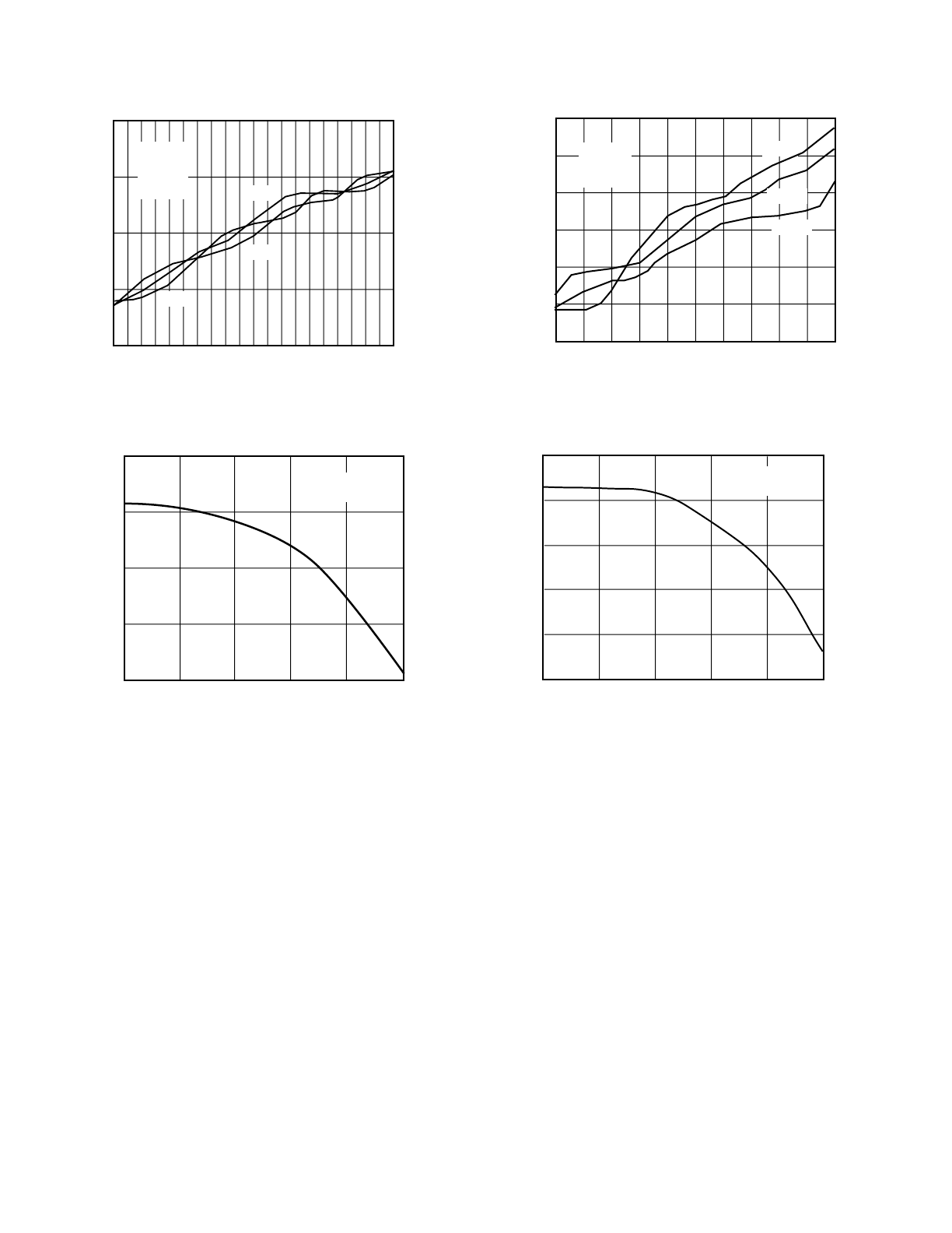
Figure 1. On Resistance as a Function of V
D
(V
S
) Dual
Supplies
50
0
30
10
20
40
R
ON
–
V
D
OR V
S
– DRAIN OR SOURCE VOLTAGE – V
–5
5
–4
3
4
2
1
0
–1
–2
–3
V
DD
= +5V
V
SS
= –5V
+125
°
C
+85
°
C
+25
°
C
Ω
Figure 2. On Resistance as a Function of V
D
(V
S
) for
Different Temperatures
Typical Performance Graphs–ADG511/ADG512/ADG513
REV. 0
–7–
R
ON
–
V
D
OR V
S
– DRAIN OR SOURCE VOLTAGE – V
90
20
5
50
30
1
40
0
80
60
70
4
3
2
V
DD
= +5V
V
SS
= 0V
V
DD
= +3V
V
SS
= 0V
T
A
= +25
°
C
Ω
Figure 3. On Resistance as a Function of V
D
(V
S
)
Single Supply
10nA
100nA
1µA
10µA
100µA
100k
10M
100
1k
10k
1M
FREQUENCY – Hz
10
1mA
10mA
I
SUPPLY
V
DD
= +5V
V
SS
= –5V
I–, I+
1 SW
4 SW
Figure 4. Supply Current vs. Input Switching Frequency
LEAKAGE CURRENT – nA
10
0.001
25
125
1
0.01
35
0.1
105
115
95
85
75
65
55
45
I
D
(ON)
I
S
(OFF)
I
D
(OFF)
V
DD
= +5V
V
SS
= –5V
V
S
= ±5V
V
D
= 5V
TEMPERATURE –
°
C
±
Figure 5. Leakage Currents as a Function of Temperature
40
60
80
100
120
100
1k
10k
100k
1M
10M
FREQUENCY – Hz
OFF ISOLATION – dB
V
DD
= +5V
V
SS
= –5V
Figure 6. Off Isolation vs. Frequency
ADG511/ADG512/ADG513–Typical Performance Graphs
REV. 0
–8–
LEAKAGE CURRENT – nA
V
D
or V
S
– DRAIN OR SOURCE VOLTAGE – V
0.006
–0.006
5
0.000
–0.004
–4
–0.002
–5
0.004
0.002
4
2
1
0
3
–1
–2
–3
I
D
(ON)
I
S
(OFF)
I
D
(OFF)
V
DD
= +5V
V
SS
= –5V
T
A
= +25
°
C
Figure 7. Leakage Currents as a Function of V
D
(V
S
)
100
1k
10k
100k
1M
10M
60
70
80
90
100
110
FREQUENCY – Hz
CROSSTALK – dB
V
DD
= +5V
V
SS
= –5V
Figure 8. Crosstalk vs. Frequency
ADG511/ADG512/ADG513
REV. 0
–9–
TRENCH ISOLATION
In the ADG511/ADG512/ADG513, an insulating oxide layer
(trench) is placed between the NMOS and the PMOS transis-
tors of each CMOS switch. Parasitic junctions, which occur be-
tween the transistors in Junction Isolated switches, are
eliminated. The result is a completely latch-up proof switch.
In Junction Isolation, the N and P wells of the PMOS and
NMOS transistors form a diode which is reverse-biased under
normal operation. However, during overvoltage conditions, this
diode becomes forward biased. A Silicon-Controlled Rectifier
(SCR) type circuit is formed by the two transistors causing a
significant amplification of the current which, in turn, leads to
latch-up. With Trench Isolation, this diode is removed, the re-
sult being a latch-up proof switch.
Trench Isolation also leads to lower leakage currents. The
ADG511/ADG512/ADG513 has a leakage current of 0.1 nA as
compared with a leakage current of several nanoamps in non-
Trench Isolated switches. Leakage current is an important
parameter in sample-and-hold circuits, this current being
responsible for the discharge of the holding capacitor with time
causing droop. The ADG511/ADG512/ADG513’s low leakage
current, along with its fast switching speeds, make it suitable for
fast and accurate sample-and-hold circuits.
AA
AA
AA
AA
AA
AA
AA
AA
AA
AA
AAAA
AAAA
AAAA
AAAA
AAAA
AAAA
A
A
A
A
A
AAAAAAAAA
AAAAAAAAA
AAA
AAA
AA
AA
AA
AA
AA
AA
AA
AA
AA
AA
AA
AA
AA
AA
AA
AA
LOCOS
NMOS
PMOS
n - WELL
AAA
AAA
TRENCH
AAAAA
AAAAA
SUBSTRATE (BACKGATE)
AAA
AAA
p - WELL
AAAAA
AAAAA
BURIED OXIDE LAYER
Figure 9. Trench Isolation
APPLICATION
Figure 10 illustrates a precise sample-and-hold circuit. An
AD845 is used as the input buffer while the output operational
amplifier is an OP07. During the track mode, SW1 is closed and
the output V
OUT
follows the input signal V
IN
. In the hold mode,
SW1 is opened and the signal is held by the hold capacitor C
H
.
Due to switch and capacitor leakage, the voltage on the hold ca-
pacitor will decrease with time. The ADG511/ADG512/ADG513
minimizes this droop due to its low leakage specifications. The
droop rate is further minimized by the use of a polystyrene
hold capacitor. The droop rate for the circuit shown is typically
15
µ
V/
µ
s.
A second switch SW2, which operates in parallel with SW1, is
included in this circuit to reduce pedestal error. Since both
switches will be at the same potential, they will have a differen-
tial effect on the op amp OP07 which will minimize charge in-
jection effects. Pedestal error is also reduced by the compensation
network R
C
and C
C
. This compensation network also reduces
the hold time glitch while optimizing the acquisition time. Using
the illustrated op amps and component values, the pedestal er-
ror has a maximum value of 5 mV over the
±
3 V input range.
The acquisition time is 2.5
µ
s while the settling time is 1.85
µ
s.
+5V
–5V
AD84
5
13
ADG511/
512/513
+5V
5
4
SW1
SW2
–5V
S
D
S
D
V
IN
+5V
–5V
V
OUT
2200pF
OP-07
C
C
1000pF
R
C
75
C
H
2200pF
Ω
Figure 10. Accurate Sample-and-Hold
ADG511/ADG512/ADG513
REV. 0
–10–
Test Circuits
S
D
V
S
V1
R
ON
= V
1
/I
DS
I
DS
Test Circuit 1. On Resistance
S
D
V
S
A
A
V
D
I
D
(OFF)
I
S
(OFF)
Test Circuit 2. Off Leakage
S
D
A
V
D
I
D
(ON)
V
S
Test Circuit 3. On Leakage
S
D
V
S
IN
GND
V
SS
R
L
300
Ω
C
L
35pF
V
OUT
V
DD
V
DD
0.1µF
V
SS
0.1µF
3V
3V
t
ON
t
OFF
90%
90%
50%
50%
50%
50%
V
IN
V
IN
V
OUT
ADG511
ADG512
Test Circuit 4. Switching Times
ADG511/ADG512/ADG513
REV. 0
–11–
IN1, IN2
GND
V
SS
V
DD
V
DD
0.1µF
V
SS
0.1µF
V
IN
S2
V
S2
D2
V
OUT2
R
L2
300
Ω
C
L2
35pF
S1
V
S1
D1
V
OUT1
R
L1
300
Ω
C
L1
35pF
3V
3V
t
D
t
D
90%
90%
90%
90%
50%
50%
V
IN
V
OUT1
V
OUT2
0V
0V
0V
Test Circuit 5. Break-Before-Make Time Delay
S
D
V
S
IN
GND
V
SS
C
L
10nF
V
OUT
V
DD
V
DD
V
SS
R
S
3V
V
IN
V
OUT
V
OUT
Q
INJ
= C
L
X
V
OUT
Test Circuit 6. Charge Injection
V
OUT
S
D
V
S
GND
V
SS
R
L
50
Ω
V
DD
V
DD
0.1µF
V
SS
0.1µF
V
IN1
V
IN2
50
Ω
NC
D
S
CHANNEL-TO-CHANNEL
CROSSTALK
= 20 X LOG V
S
/V
OUT
Test Circuit 8. Channel-to-Channel Crosstalk
S
D
V
S
IN
GND
V
SS
R
L
50
Ω
V
OUT
V
DD
V
DD
0.1µF
V
SS
0.1µF
V
IN
Test Circuit 7. Off Isolation
ADG511/ADG512/ADG513
REV. 0
–12–
C1750–18–4/93
PRINTED IN U.S.A.
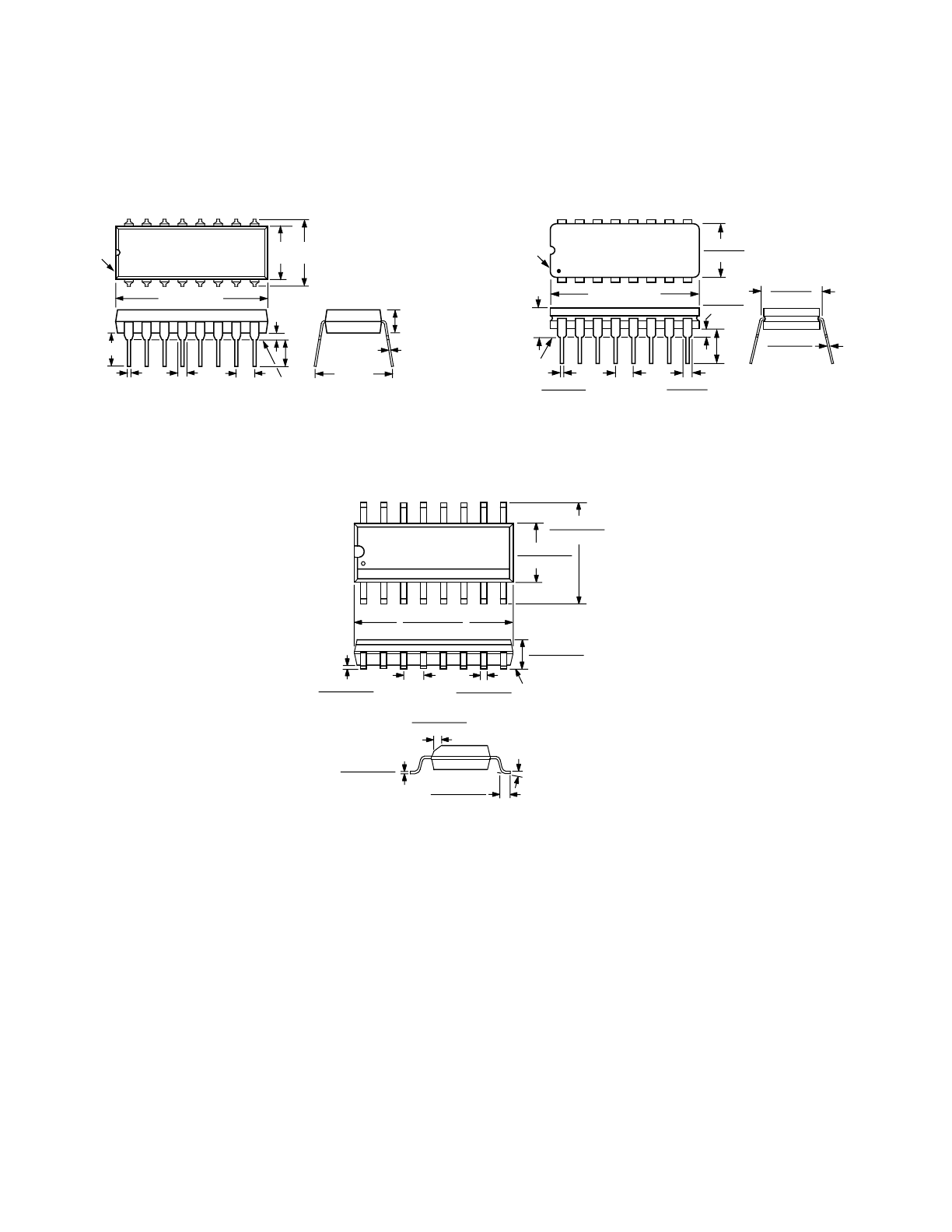
MECHANICAL INFORMATION
Dimensions are shown in inches and (mm).
16-Pin Plastic DIP
(N-16)
PIN 1
SEATING
PLANE
0.87 (22.1) MAX
1
8
9
16
0.018 (0.46)
0.033 (0.84)
0.1 (2.54)
BSC
0.011
(0.28)
0.18
(4.57)
MAX
0.3 (7.62)
0.125
(3.18)
MIN
0.035
(0.89)
0.18 (4.57)
0.25
(6.35)
0.31
(7.87)
16-Pin Cerdip
(Q-16)
PIN 1
0.840 (21.34) MAX
0.060 (1.52)
0.015 (0.38)
0.015 (0.381)
0.008 (0.204)
0.150
(3.81)
MIN
0.200
(5.08)
MAX
0.022 (0.558)
0.014 (0.356)
0.100 (2.54)
BSC
0.070 (1.78)
0.30 (0.76)
PLANE
SEATING
0.310 (7.87)
0.220 (5.59)
0.320 (8.13)
0.290 (7.37)
1
8
9
16
16-Pin SOIC
(R-16A)
×
45
°
0.0500 (1.27)
BSC
SEATING
PLANE
8
9
16
1
0.0098 (0.25)
0.0040 (0.10)
0.0192 (0.49)
0.0138 (0.35)
0.0688 (1.75)
0.0532 (1.35)
0.3937 (10.00)
0.3859 (9.80)
0.2440 (6.20)
0.2284 (5.80)
0.1574 (4.00)
0.1497 (3.80)
0
°
– 8
°
0.0099 (0.25)
0.0075 (0.19)
0.0500 (1.27)
0.0160 (0.41)
0.0196 (0.50)
0.0099 (0.25)