
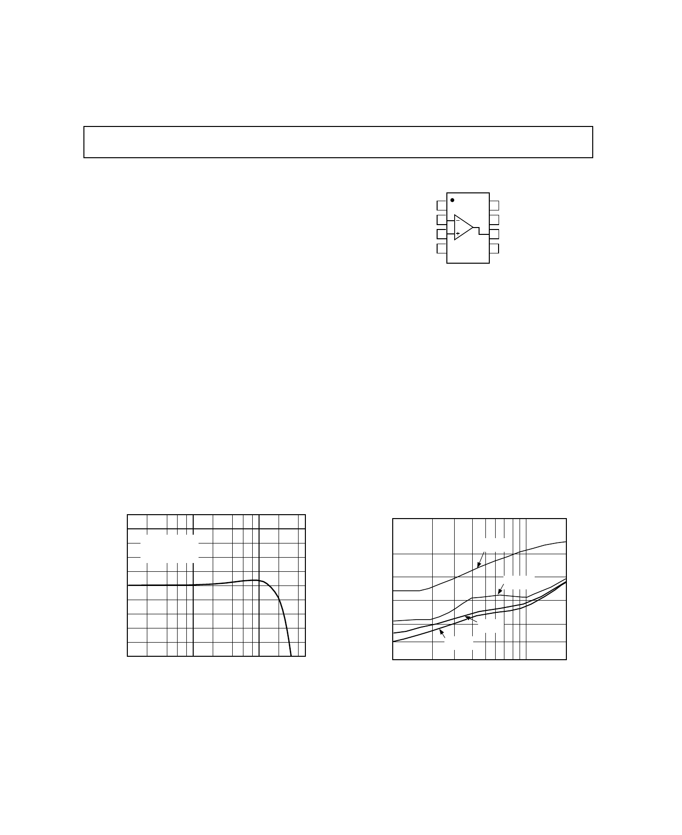
FUNCTIONAL BLOCK DIAGRAM
8-Pin Plastic Mini-DIP and SOIC
REV. 0
Information furnished by Analog Devices is believed to be accurate and
reliable. However, no responsibility is assumed by Analog Devices for its
use, nor for any infringements of patents or other rights of third parties
which may result from its use. No license is granted by implication or
otherwise under any patent or patent rights of Analog Devices.
a
300 MHz, 1 mA
Current Feedback Amplifier
AD8011*
FEATURES
Easy to Use
Low Power
1 mA Power Supply Current (5 mW on +5 V
S
)
High Speed and Fast Settling on +5 V
300 MHz, –3 dB Bandwidth (G = +1)
180 MHz, –3 dB Bandwidth (G = +2)
2000 V/
µ
s Slew Rate
29 ns Settling Time to 0.1%
Good Video Specifications (R
L
= 1 k
Ω
, G = +2)
Gain Flatness 0.1 dB to 25 MHz
0.02% Differential Gain Error
0.06
°
Differential Phase Error
Low Distortion
–70 dBc Worst Harmonic @ 5 MHz
–62 dBc Worst Harmonic @ 20 MHz
Single Supply Operation
Fully Specified for +5 V Supply
APPLICATIONS
Power Sensitive, High Speed Systems
Video Switchers
Distribution Amplifiers
A-to-D Driver
Professional Cameras
CCD Imaging Systems
Ultrasound Equipment (Multichannel)
+4
+3
+2
+1
0
–2
–3
–4
1 10 100 500
FREQUENCY – MHz
–1
+5
–5
NORMALIZED GAIN – dB
G = +2
R
F
= 1k
Ω
V
S
= +5V OR
±
5V
V
OUT
= 200mV p-p
Figure 1. Frequency Response; G = +2, V
S
= +5 V or
±
5 V
*Patent pending.
1
2
3
4
8
7
6
5
AD8011
NC
V+
NC
–IN
V–
NC
+IN
NC = NO CONNECT
OUT
3rd
R
L
=1k
Ω
3rd
R
L
= 150
Ω
2nd
R
L
= 150
Ω
FREQUENCY – MHz
DISTORTION – dBc
–40
–100
1
10
20
2nd
R
L
= 1k
Ω
G = +2
–60
–80
Figure 2. Distortion vs. Frequency; V
S
=
±
5 V
© Analog Devices, Inc., 1995
One Technology Way, P.O. Box 9106, Norwood. MA 02062-9106, U.S.A.
Tel: 617/329-4700
pose amplifier. It also can be used to replace high speed am-
plifiers consuming more power. The AD8011 is a current feed-
back amplifier and features gain flatness of 0.1 dB to 25 MHz
while offering differential gain and phase error of 0.02% and
0.06
°
on a single +5 V supply. This makes the AD8011 ideal
for professional video electronics such as cameras, video switch-
ers or any high speed portable equipment. Additionally, the
AD8011’s low distortion and fast settling make it ideal for
buffering high speed 8-, 10-, 12-bit A-to-D converters.
The AD8011 offers very low power of 1 mA max and can run
on single +5 V to +12 V supplies. All this is offered in a small
8-pin DIP or 8-pin SOIC package. These features fit well with
portable and battery powered applications where size and power
are critical.
The AD8011 is available in the industrial temperature range of
–40
°
C to +85
°
C.
PRODUCT DESCRIPTION
The AD8011 is a very low power, high speed amplifier designed
to operate on +5 V or
±
5 V supplies. With wide bandwidth, low
distortion and low power, this device is ideal as a general pur-

AD8011–SPECIFICATIONS
DUAL SUPPLY
Model
AD8011A
Conditions
Min
Typ
Max
Units
DYNAMIC PERFORMANCE
–3 dB Small Signal Bandwidth, V
O
< 1 V p-p
G = +1
340
400
MHz
–3 dB Small Signal Bandwidth, V
O
< 1 V p-p
G = +2
180
210
MHz
–3 dB Large Signal Bandwidth, V
O
= 5 V p-p
G = +10, R
F
= 500
Ω
57
MHz
Bandwidth for 0.1 dB Flatness
G = +2
20
25
MHz
Slew Rate
G = +2, V
O
= 4 V Step
3500
V/
µ
s
G = –1, V
O
= 4 V Step
1100
V/
µ
s
Settling Time to 0.1%
G = +2, V
O
= 2 V Step
25
ns
Rise and Fall Time
G = +2, V
O
= 2 V Step
0.4
ns
G = –1, V
O
= 2 V Step
3.7
ns
NOISE/HARMONIC PERFORMANCE
2nd Harmonic
f
C
= 5 MHz, V
O
= 2 V p-p, G = +2
R
L
= 1 k
Ω
–75
dB
R
L
= 150
Ω
–67
dB
3rd Harmonic
R
L
= 1 k
Ω
–70
dB
R
L
= 150
Ω
–54
dB
Input Voltage Noise
f = 10 kHz
2
nV/
√
Hz
Input Current Noise
f = 10 kHz, +In
5
pA/
√
Hz
–In
5
pA/
√
Hz
Differential Gain Error
NTSC, G = +2, R
L
= 1 k
Ω
0.02
%
R
L
= 150
Ω
0.02
%
Differential Phase Error
NTSC, G = +2, R
L
= 1 k
Ω
0.06
Degrees
R
L
= 150
Ω
0.3
Degrees
DC PERFORMANCE
Input Offset Voltage
2
5
±
mV
T
MIN
–T
MAX
2
6
±
mV
Offset Drift
10
µ
V/
°
C
–Input Bias Current
5
15
±µ
A
T
MIN
–T
MAX
20
±µ
A
+Input Bias Current
5
15
±µ
A
T
MIN
–T
MAX
20
±µ
A
Open-Loop Transresistance
800
1300
k
Ω
T
MIN
–T
MAX
550
k
Ω
INPUT CHARACTERISTICS
Input Resistance
+Input
450
k
Ω
Input Capacitance
+Input
2.3
pF
Input Common-Mode Voltage Range
3.8
4.1
±
V
Common-Mode Rejection Ratio
Offset Voltage
V
CM
=
±
2.5 V
–52
–57
dB
OUTPUT CHARACTERISTICS
Output Voltage Swing
3.9
4.1
±
V
Output Resistance
0.1
0.3
Ω
Output Current
T
MIN
–T
MAX
15
30
mA
Short Circuit Current
60
mA
POWER SUPPLY
Operating Range
±
1.5
±
6.0
V
Quiescent Current
T
MIN
–T
MAX
1.0
1.2
mA
Power Supply Rejection Ratio
Vs =
±
5 V
±
1 V
55
58
dB
Specifications subject to change without notice.
REV. 0
–2–
(@ T
A
= +25
°
C, V
S
=
±
5 V, G = +2, R
F
= 1 k
Ω
, R
L
= 1 k
Ω
, unless otherwise noted)

SINGLE SUPPLY
Model
AD8011A
Conditions
Min
Typ
Max
Units
DYNAMIC PERFORMANCE
–3 dB Small Signal Bandwidth, V
O
< 0.5 V p-p
G = +1
270
328
MHz
–3 dB Small Signal Bandwidth, V
O
< 0.5 V p-p
G = +2
150
180
MHz
–3 dB Large Signal Bandwidth, V
O
= 2.5 V p-p
G = +10, R
F
= 500
Ω
57
MHz
Bandwidth for 0.1 dB Flatness
G = +2
15
20
MHz
Slew Rate
G = +2, V
O
= 2 V Step
2000
V/
µ
s
G = –1, V
O
= 2 V Step
500
V/
µ
s
Settling Time to 0.1%
G = +2, V
O
= 2 V Step
29
ns
Rise and Fall Time
G = +2, V
O
= 2 V Step
0.6
ns
G = –1, V
O
= 2 V Step
4
ns
NOISE/HARMONIC PERFORMANCE
2nd Harmonic
f
C
= 5 MHz, V
O
= 2 V p-p, G = +2
R
L
= 1 k
Ω
–84
dB
R
L
= 150
Ω
–67
dB
3rd Harmonic
R
L
= 1 k
Ω
–76
dB
R
L
= 150
Ω
–54
dB
Input Voltage Noise
f = 10 kHz
2
nV/
√
Hz
Input Current Noise
f = 10 kHz, +In
5
pA/
√
Hz
–In
5
pA/
√
Hz
Differential Gain Error
NTSC, G = +2, R
L
= 1 k
Ω
0.02
%
R
L
= 150
Ω
0.6
%
Differential Phase Error
NTSC, G = +2, R
L
= 1 k
Ω
0.06
Degrees
R
L
= 150
Ω
0.8
Degrees
DC PERFORMANCE
Input Offset Voltage
2
5
mV
T
MIN
–T
MAX
2
6
mV
Offset Drift
10
µ
V/
°
C
–Input Bias Current
5
15
±µ
A
T
MIN
–T
MAX
20
±µ
A
+Input Bias Current
5
15
±µ
A
T
MIN
–T
MAX
20
±µ
A
Open-Loop Transresistance
800
1300
k
Ω
T
MIN
–T
MAX
550
k
Ω
INPUT CHARACTERISTICS
Input Resistance
+Input
450
k
Ω
Input Capacitance
+Input
2.3
pF
Input Common-Mode Voltage Range
1.5 to 3.5
1.2 to 3.8
V
Common-Mode Rejection Ratio
Offset Voltage
V
CM
= 1.5 V to 3.5 V
–52
–57
dB
OUTPUT CHARACTERISTICS
Output Voltage Swing
1.2 to 3.8
0.9 to 4.1
+V
Output Resistance
0.1
0.3
Ω
Output Current
T
MIN
–T
MAX
15
30
mA
Short Circuit Current
50
mA
POWER SUPPLY
Operating Range
+3
+12
V
Quiescent Current
T
MIN
–T
MAX
0.8
1.0
mA
Power Supply Rejection Ratio
∆
Vs =
±
1 V
55
58
dB
Specifications subject to change without notice.
REV. 0
–3–
AD8011
(@ T
A
= +25
°
C, V
S
= +5 V, G = +2, R
F
= 1 k
Ω
, V
CM
= 2.5 V, R
L
= 1 k
Ω
, unless otherwise noted)
REV. 0
–4–
AD8011
ABSOLUTE MAXIMUM RATINGS
1
Supply Voltage . . . . . . . . . . . . . . . . . . . . . . . . . . . . . . . . 12.6 V
Internal Power Dissipation
2
Plastic Package (N) . . . . . . . . . . . . Observe Derating Curves
Small Outline Package (R) . . . . . . . Observe Derating Curves
Input Voltage (Common Mode) . . . . . . . . . . . . . . . . . . . .
±
V
S
Differential Input Voltage . . . . . . . . . . . . . . . . . . . . . . .
±
2.5 V
Output Short Circuit Duration
. . . . . . . . . . . . . . . . . . . . . . Observe Power Derating Curves
Storage Temperature Range (N, R) . . . . . . . . –65
°
C to +125
°
C
Operating Temperature Range (A Grade) . . . – 40
°
C to +85
°
C
Lead Temperature Range (Soldering 10 sec) . . . . . . . . +300
°
C
NOTES
1
Stresses above those listed under “Absolute Maximum Ratings” may cause
permanent damage to the device. This is a stress rating only and functional
operation of the device at these or any other conditions above those indicated in the
operational section of this specification is not implied. Exposure to absolute
maximum rating conditions for extended periods may affect device reliability.
2
Specification is for device in free air:
8-Pin Plastic Package:
θ
JA
= 90
°
C/Watt
8-Pin SOIC Package:
θ
JA
= 140
°
C/Watt
ORDERING GUIDE
Model
Temperature Range
Package Option
AD8011AN
– 40
°
C to +85
°
C
8-Pin Plastic DIP
AD8011AR
– 40
°
C to +85
°
C
8-Pin SOIC
AD8011-EB
Eval Board, SOIC,
G = +2
MAXIMUM POWER DISSIPATION
The maximum power that can be safely dissipated by the
AD8011 is limited by the associated rise in junction tempera-
ture. The maximum safe junction temperature for plastic
encapsulated devices is determined by the glass transition tem-
perature of the plastic, approximately +150
°
C. Exceeding this
limit temporarily may cause a shift in parametric performance
due to a change in the stresses exerted on the die by the package.
Exceeding a junction temperature of +175
°
C for an extended
period can result in device failure.
While the AD8011 is internally short circuit protected, this
may not be sufficient to guarantee that the maximum junction
temperature is not exceeded under all conditions. To ensure
proper operation, it is necessary to observe the maximum power
derating curves (shown below in Figure 3).
2.0
1.5
0.5
–50 –40 –30 –20 –10
0
10
20 30
40
50
60 70
80 90
AMBIENT TEMPERATURE –
°
C
1.0
0
MAXIMUM POWER DISSIPATION – Watts
T
J
= +150
°
C
8-PIN MINI-DIP PACKAGE
8-PIN SOIC PACKAGE
Figure 3. Maximum Power Dissipation vs. Temperature
WARNING!
ESD SENSITIVE DEVICE
CAUTION
ESD (electrostatic discharge) sensitive device. Electrostatic charges as high as 4000 V readily
accumulate on the human body and test equipment and can discharge without detection.
Although the AD8011 features proprietary ESD protection circuitry, permanent damage may
occur on devices subjected to high energy electrostatic discharges. Therefore, proper ESD
precautions are recommended to avoid performance degradation or loss of functionality.
AD8011
REV. 0
–5–
52.3
Ω
0.01µF
0.01µF
10µF
10µF
R
L
1k
Ω
1k
Ω
1k
Ω
V
IN
V
OUT
+V
S
–V
S
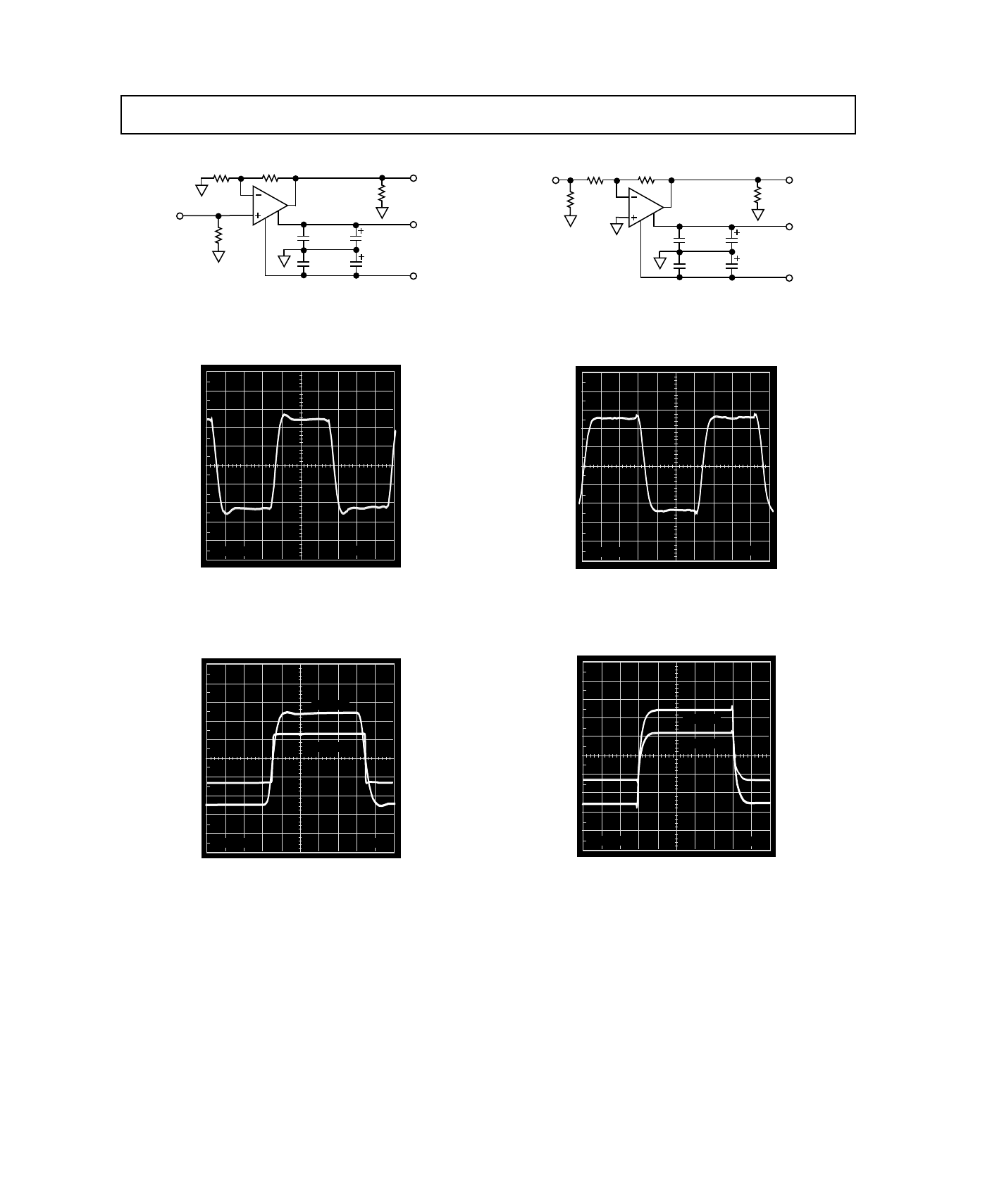
Figure 7. Test Circuit; Gain = –1
20mV
5ns
Figure 8.* 100 mV Step Response; G = –1, V
S
=
±
2.5 V or
±
5 V
800mV
10ns
4V STEP
2V STEP
Figure 9.* Step Response; G = –1, V
S
=
±
2.5 V (2 V
Step) and
±
5 V (4 V Step)
0.01µF
0.01µF
10µF
10µF
R
L
1k
Ω
1k
Ω
1k
Ω
50
Ω
V
IN
V
OUT
+V
S
–V
S
Figure 4. Test Circuit; Gain = +2
20mV
5ns
Figure 5.* 100 mV Step Response; G = +2, V
S
=
±
2.5 V or
±
5 V
800mV
10ns
4V STEP
2V STEP
Figure 6.* Step Response; G = +2, V
S
=
±
2.5 V (2 V
Step) and
±
5 V (4 V Step)
*NOTE: V
S
=
±
2.5 V operation is identical to V
S
= +5 V single supply operation.
REV. 0
–6–
AD8011
6.5
6.4
6.3
6.2
6.1
5.9
5.8
5.7
1 10 100 500
FREQUENCY – MHz
6.0
5.6
5.5
GAIN – dB
V
S
=
±
5V
V
S
= 5V
G = +2
V
IN
= 100mV p-p
R
L
= 1k
Ω
R
F
= 1k
Ω
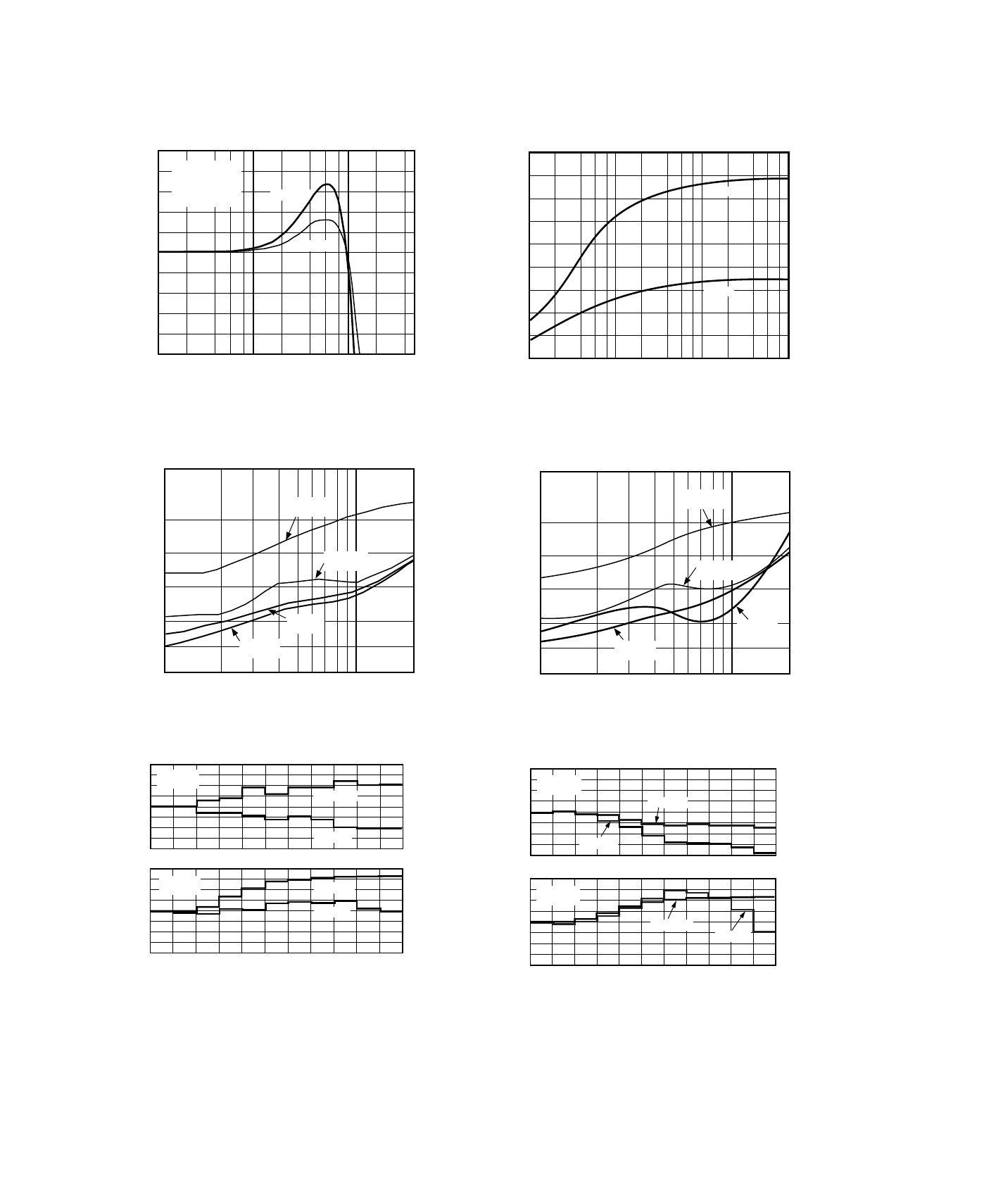
Figure 10. Gain Flatness; G = +2
3rd
R
L
=1k
Ω
3rd
R
L
= 150
Ω
2nd
R
L
= 150
Ω
FREQUENCY – MHz
DISTORTION – dBc
–40
–100
1
10
20
2nd
R
L
= 1k
Ω
G = +2
–60
–80
Figure 11. Distortion vs. Frequency; V
S
=
±
5 V
1k
Ω
DIFF PHASE – Degrees
100
0
IRE
R
L
= 1k
Ω
DIFF GAIN – %
R
L
= 150
Ω
R
L
= 150
Ω
100
0
IRE
R
L
= 1k
Ω
0.04
–0.04
0.00
–0.02
0.02
0.01
–0.01
–0.03
0.03
0.04
–0.04
0.00
–0.02
0.02
0.01
–0.01
–0.03
0.03
V
S
=
±
5V
G = +2
V
S
=
±
5V
G = +2
0.4
–0.4
0.00
–0.2
0.2
150
Ω
DIFF PHASE – Degrees
0.1
–0.1
–0.3
0.3
Figure 12. Diff Phase and Diff Gain; V
S
=
±
5 V
9
8
7
6
5
3
2
10 100 1000 10000
LOAD RESISTANCE – Ohms
4
1
0
SWING – V p
-p
+5V
±
5V
Figure 13. Output Voltage Swing vs. Load
3rd
R
L
=1k
Ω
3rd
R
L
=150
Ω
FREQUENCY – MHz
DISTORTION – dBc
–40
–100
1
10
20
2nd
R
L
=150
Ω
2nd
R
L
=1k
Ω
G = +2
–60
–80
Figure 14. Distortion vs. Frequency; V
S
= +5 V
0.08
1k
Ω
DIFF GAIN – %
–0.08
0.00
–0.04
0.04
100
0
IRE
1k
Ω
DIFF PHASE – Degrees
150
Ω
DIFF PHASE – Degrees
100
0
IRE
0.02
–0.02
–0.06
0.06
0.8
–0.8
0.0
–0.4
0.4
0.2
–0.2
–0.6
0.6
0.08
–0.08
0.00
–0.04
0.04
0.02
–0.02
–0.06
0.06
R
L
=150
Ω
R
L
=1k
Ω
R
L
=1k
Ω
R
L
=150
Ω
V
S
= +5V
G = +2
V
S
= +5V
G = +2
150
Ω
DIFF GAIN – %
0.8
–0.8
0.0
–0.4
0.4
0.2
–0.2
–0.6
0.6
Figure 15. Diff Phase and Diff Gain; V
S
= +5 V
AD8011
REV. 0
–7–
0
–3
–6
–9
–12
–18
–21
–24
1 10 40 100 500
FREQUENCY – MHz
–15
+3
OUTPUT VOLTAGE – dBV
–27
1V rms
Figure 19. Large Signal Frequency Response;
V
S
= +5 V, G = +2
0.1%
5ns
G = +2
R
F
= 1k
Ω
2V STEP
t
= 0
OUTPUT VOLTAGE – 0.1%/DIV
Figure 20. Short-Term Settling Time; V
S
= +5 V or
±
5 V
0.1%
100ns
G = +2
R
F
= 1k
Ω
2V STEP
t
= 0
OUTPUT VOLTAGE – 0.1%/DIV
Figure 21. Long-Term Settling Time; V
S
= +5 V or
±
5 V
+6
+3
0
–3
–6
–12
–15
–18
1 10 40 100 500
FREQUENCY – MHz
–9
+9
OUTPUT VOLTAGE – dBV
–21
1V rms
Figure 16. Large Signal Frequency Response;
V
S
=
±
5 V, G = +2
+4
+3
+2
+1
0
–2
–3
–4
1 10 100 500
FREQUENCY – MHz
–1
+5
NORMALIZED GAIN – dB
–5
G = +1
R
F
= 1k
Ω
G = +10
R
F
= 500
Ω
G = +2
R
F
= 1k
Ω
V
S
= +5V OR
±
5V
V
OUT
= 200mV p-p
Figure 17. Frequency Response; G = +1, +2, +10;
V
S
= +5 V or
±
5 V
+1
0
–2
–3
–4
1 10 100 500
FREQUENCY – MHz
–1
+2
NORMALIZED GAIN – dB
–5
–6
–7
–8
G = –10
R
F
= 500
Ω
R
L
= 1k
Ω
V
S
= +5V OR
±
5V
V
OUT
= 200mV p-p
G = –1
R
F
= 1k
Ω
R
L
= 1k
Ω
Figure 18. Frequency Response; G = –1, –10;
V
S
= +5 V or
±
5 V
REV. 0
–8–
AD8011
–10
–15
–20
–25
–30
–40
–45
–50
0.1 1 10 100
FREQUENCY – MHz
–35
–55
–60
CMRR – dB
V
S
= +5V OR
±
5V
G = +2
Figure 22. CMRR vs. Frequency; V
S
= +5 V or
±
5 V
100
10
0.1
10k 0.1M 1M 10M 100M 500M
FREQUENCY – Hz
1
0.01
OUTPUT RESISTANCE –
Ω
V
S
= +5V OR
±
5V
G = +2
R
F
= 1k
Ω
Figure 23. Output Resistance vs. Frequency; V
S
= +5 V
or
±
5 V
1k 10k 100k 1M 10M 100M 1G
140
120
100
80
60
20
0
FREQUENCY – Hz
40
GAIN – dB Ohms
0
PHASE – Degrees
–40
–80
–120
–160
–200
–240
–280
PHASE
GAIN
Figure 24. Transimpedance Gain and Phase vs. Frequency
+10
0
–10
–20
–30
–50
–60
–70
100k 1M 10M 100M 500M
FREQUENCY – Hz
–40
–80
–90
PSRR – dB
V
S
= +5V OR
±
5V
G = +2
R
F
= 1k
Ω
+PSRR
–PSRR
Figure 25. PSRR vs. Frequency; V
S
= +5 V or
±
5 V
12.5
10
5
2.5
500 1k 10k 100k
FREQUENCY – Hz
7.5
0
INPUT VOLTAGE NOISE – nV/
√
Hz
INPUT CURRENT NOISE – pA/
√
Hz
50
40
20
10
30
0
Figure 26. Noise vs. Frequency; V
S
= +5 V or
±
5 V
9
8
7
6
5
4
3
2
3 4 5 6 7 8 9 10 11
1
0
f = 5MHz
G = +2
R
F
= 1k
Ω
R
L
= 150
Ω
R
L
= 1k
Ω
TOTAL SUPPLY VOLTAGE – V
PEAK-TO-PEAK OUTPUT AT 5MHz (
≤
0.5% THD) – V
Figure 27. Output Swing vs. Supply
AD8011
REV. 0
–9–
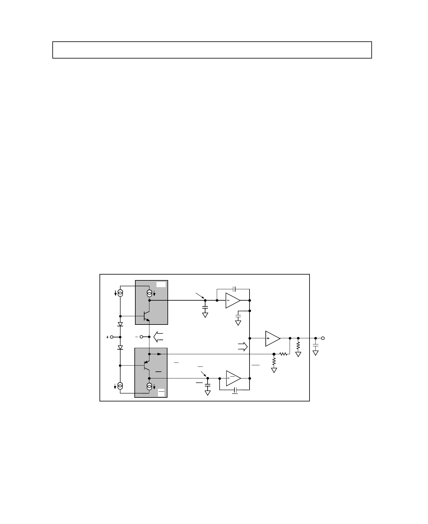
THEORY OF OPERATION
The AD8011 is a revolutionary generic high speed CF amplifier
that attains new levels of BW, power, distortion, and signal
swing capability. If these key parameters were combined as a fig-
ure of ac merit performance or [(frequency
×
V
SIG
)/(distortion
×
power)], no IC amplifier today would come close to the merit
value of the AD8011 for frequencies above a few MHz. Its wide
dynamic performance (including noise) is the result of both a
new complementary high speed bipolar process and a new and
unique architectural design. The AD8011 uses basically a two
gain stage complementary design approach versus the traditional
“single stage” complementary mirror structure sometimes re-
ferred to as the Nelson amplifier. Though twin stages have been
tried before, they typically consumed high power since they
were of a folded cascade design much like the AD9617. This de-
sign allows for the standing or quiescent current to add to the
high signal or slew current induced stages much like the Nelson
or single stage design. Thus, in the time domain, the large signal
output rise/fall time and slew rate is controlled typically by the
small signal BW of the amplifier and the input signal step ampli-
tude respectively, not the dc quiescent current of the gain stages
(with the exception of input level shift diodes Q1/Q2). Using
two stages vs. one also allows for a higher overall gain band-
width product (GBWP) for the same power, thus lower signal
distortion and the ability to drive heavier external loads. In addi-
tion, the second gain stage also isolates (divides down) A3’s in-
put reflected load drive and the nonlinearities created resulting
in relatively lower distortion and higher open-loop gain.
Overall, when “high” external load drive and low ac distortion is
a requirement, a twin gain stage integrating amplifier like the
AD8011 will provide superior results for lower power over the
traditional single stage complementary devices. In addition, be-
ing a CF amplifier, closed-loop BW variations versus external
gain variations (varying RN) will be much lower compared to a
VF op amp, where the BW varies inversely with gain. Another
key attribute of this amplifier is its ability to run on a single 5 V
supply due in part to its wide common-mode input and output
voltage range capability. For 5 V supply operation, the device
obviously consumes half the quiescent power (vs. 10 V supply)
with little degradation in its ac and dc performance characteris-
tics. See data sheet comparisons.
DC GAIN CHARACTERISTICS
Gain stages A1/A1B and A2/A2B combined provide negative
feedforward transresistance gain. See Figure 28. Stage A3 is a
unity gain buffer which provides external load isolation to A2.
Each stage uses a symmetrical complementary design. (A3 is
also complementary though not explicitly shown). This is done
to both reduce second order signal distortion and overall quies-
cent power as discussed above. In the quasi dc to low frequency
region, the closed loop gain relationship can be approximated as:
G = 1+R
F
/R
N
noninverting operation
G = –R
F
/R
N
inverting operation
These basic relationships above are common to all traditional
operational amplifiers. Due to the inverting input error current
(I
E
) required to servo the output and the inverting I
E
×
R
I
drop
V
P
Q1
Q2
IPP
IPN
INP
IPN
V
N
A1
A1
Z
I
IQ1
Q3
Q4
IE
IR
–
IFC
IR +
I FC
C
P
1
C
P
1
Z2
A2
C
L
R
L
ICQ
–
IO
R
F
V
O
C
D
ICQ +
IO
–V
I
–V
I
V
O
´
IQ1
AD8011
A2
C
P
2
Z1
Z1 = R1 || C1
Z1
C
D
A3
R
L
Figure 28. Simplified Block Diagram
REV. 0
–10–
AD8011
This analysis assumes perfect current sources and infinite tran-
sistor V
A
s (Q3, Q4 output conductances are assumed zero).
These assumptions result in actual vs. model open loop voltage
gain and associated input referred error terms being less accurate
for low gain (G) noninverting operation at the frequencies below
the open loop pole of the AD8011. This is primarily a result of
the input signal (V
P
) modulating the output conductances of
Q3/Q4 resulting in R
I
less negative than derived here. For invert-
ing operation, the actual vs. model dc error terms are relatively
much less.
AC TRANSFER CHARACTERISTICS
The ac small signal transfer derivations below are based on a
simplified single-pole model. Though inaccurate at frequencies
approaching the closed-loop BW (CLBW) of the AD8011 at low
noninverting external gains, they still provide a fair approximation
and a intuitive understanding of its primary ac small signal
characteristics.
For inverting operation and high noninverting gains these trans-
fer equations provide a good approximation to the actual ac
performance of the device.
To accurately quantify the V
O
vs. V
P
relationship, both A
O
(s)
and T
O
(s) need to be derived. This can be seen by the following
nonexpanded noninverting gain relationship:
V
O
(s) /V
P
(s)
=
G
G
A
O
[s]
+
R
F
T
O
[s]
+
1
with
A
O
(s)
=
R1
×
g
mf
×
|A2|
1 – g
mc
×
R1
S
τ
1
1 – g
mc
×
R1
1E+03 1E+04 1E+05 1E+06 1E+07 1E+08 1E+09
80
70
60
50
40
20
10
FREQUENCY – Hz
30
GAIN – dB Ohms
–90
PHASE – Degrees
–100
–110
–120
–160
PHASE
GAIN
0
–10
–20
–30
–170
–180
–190
–200
–130
–140
–150
A
O
(s)
Figure 30. Open-Loop Voltage Gain and Phase
(error current times the open loop inverting input resistance)
that results (see Figure 29), a more exact low frequency closed
loop transfer functions can be described as:
A
V
=
G
1
+
G
×
R
I
T
O
+
R
F
T
O
=
G
1
+
G
A
O
+
R
F
T
O
for noninverting (G is positive)
A
V
=
G
1
+
1 – G
A
O
+
R
F
T
O
for inverting (G is negative)
R
S
L
N
T
O
(s)
A
O
(s)
V
P
Z
I
IE
L
I
R
N
C
P
R
F
+V
S
–V
S
L
S
R
L
C
L
V
O
L
S
Z
I
= OPEN LOOP INPUT IMPEDANCE = C
I
|| R
L
Figure 29. Z
I
= Open-Loop Input Impedance
where G is the ideal gain as previously described. With
R
I
= T
O
/A
O
(open-loop inverting input resistance), the second
expression (positive G) clearly relates to the classical voltage
feedback “op amp” equation with T
O
omitted do to its relatively
much higher value and thus insignificant effect. A
O
and T
O
are
the open-loop dc voltage and transresistance gains of the ampli-
fier respectively. These key transfer variables can be described as:
AO
=
R1
×
gmf
×
| A2|
(1 – gmc
×
R1)
and TO
=
R1
×
| A2|
2
; therefore RI
=
1
−
g
mc
×
R1
2
×
g
mf
Where g
mc
is the positive feedback transconductance (not
shown) and 1/g
mf
is the thermal emitter resistance of devices
D1/D2 and Q3/Q4. The g
mc
×
R1 product has a design value that
results in a negative dc open loop gain of typically –2500 V/V (see
Figure 30).
Though atypical of conventional CF or VF amps, this negative
open-loop voltage gain results in an input referred error term
(V
P
–V
O
/G = G/A
O
+ R
F
/T
O
) that will typically be negative for G
greater than +3/–4. As an example, for G = 10, A
O
= –2500 and
T
O
= 1.2 M
Ω
, results in a error of –3 mV using the A
V
deriva-
tion above.
AD8011
REV. 0
–11–
1E+03 1E+04 1E+05 1E+06 1E+07 1E+08 1E+09
400
370
340
310
280
220
190
FREQUENCY – Hz
250
RESISTANCE – Ohms
20
PHASE – Degrees
0
–20
–40
–120
PHASE
IMPEDANCE
160
130
100
–140
–160
–180
–60
–80
–100
SERIES 1
SERIES 2
Z
I
(s)
Figure 32. Open-Loop Inverting Input Impedance
Z
I
(s) goes positive real and approaches 1/2 g
mf
as
ω
approaches
(g
mc
×
R1 – 1)
/τ1
. This results in the input resistance for the
A
V
(s) complex term being 1/2 g
mf
; the parallel thermal emitter
resistances of Q3/Q4. Using the computed CLBW from A
V
(s)
above and the nominal design values for the other parameters,
results in a closed loop 3 dB BW equal to the open loop corner
frequency (1/2
πτ
1) times 1/[G/(2 g
mf
×
T
O
) + R
F
/T
O
]. For a
fixed R
F
, the 3 dB BW is controlled by the R
F
/T
O
term for low
gains and G/(2 g
mf
×
T
O
) for high gains. For example, using
nominal design parameters and R
1
= 1 k
Ω
(which results in a
nominal T
O
of 1.2 M
Ω
, the computed BW is 80 MHz for G = 0
(inverting I-V mode with R
N
removed) and 40 MHz for
G = +10/–9.
DRIVING CAPACITIVE LOADS
The AD8011 was designed primarily to drive nonreactive loads.
If driving loads with a capacitive component is desired, best set-
tling response is obtained by the addition of a small series resis-
tance as shown in Figure 33. The accompanying graph shows
the optimum value for R
SERIES
vs. capacitive load. It is worth
noting that the frequency response of the circuit when driving
large capacitive loads will be dominated by the passive roll-off of
R
SERIES
and C
L
.
1k
Ω
R
L
1k
Ω
C
L
AD8011
R
SERIES
1k
Ω
Figure 33. Driving Capacitive Load
where R1 is the input resistance to A2/A2B, and
τ1
(equal to
CD
×
R1
×
A2) is the open loop dominate time constant.
and T
O
(s)
=
|A2|
×
R1
2
s
τ
1
+
1
1E+03 1E+04 1E+05 1E+06 1E+07 1E+08 1E+09
140
120
100
80
60
20
0
FREQUENCY – Hz
40
GAIN – dB Ohms
0
PHASE – Degrees
–40
–80
–120
–160
–200
–240
–280
PHASE
GAIN
T
O
(s)
Figure 31. Open-Loop Transimpedance Gain
Note that the ac open-loop plots in Figures 31, 32 and 33 are
based on the full Spice AD8011 simulations and do not include
external parasitics (see below). Nevertheless, these ac loop equa-
tions still provide a good approximation to simulated and actual
performance up to the CLBW of the amplifier. Typically g
mc
×
R1 is –4, resulting in A
O
(s) having a right half plane pole. In the
time domain (inverse Laplace of A
O
) it appears as unstable,
causing V
O
to exponentially rail out of its linear region. When
the loop is closed however, the BW is greatly extended and the
transimpedance gain, T
O
(s) “overrides” and directly controls
the amplifiers stability behavior due to Z
I
approaching 1/2 g
mf
for s>>1/
τ
1. See Figure 32. This can be seen by the Z
I
(s) and A
V
(s) noninverting transfer equations below.
Z
I
(s)
=
(1 – g
mc
×
R1)
S
τ
1
1 – g
mc
×
R1
+
1
2
×
g
mf
( S
τ
1
+
1)
A
V
(s)
=
G
1
+
G
A
O
+
R
F
T
O
S
τ
1
G
2 g
mf
T
O
+
R
F
T
O
+
1
REV. 0
–12–
AD8011
11
10
9
8
7
5
4
3
6
2
1
1 10 100 500
FREQUENCY – MHz
GAIN – dB
R
F
= 1k
Ω
R
F
= 750
Ω
V
S
=
±
5V
G = +2
V
IN
= 200mV
Figure 35. Flatness vs. Feedback
Output pin and external component capacitance (designated
C
L
) will further extend the devices BW and can also cause peak-
ing below and above the CLBW if too high. In the time domain,
poor step settling characteristics (ringing up to about 2 GHz
and excessive overshoot) can result. For high C
L
values greater
than about 5 pF an external series “damping” resistor is recom-
mended. See section on Settling Time vs. C
L
. For light loads,
any output capacitance will reflect back on A2’s output (Z2 of
buffer A3) as both added capacitance near the CLBW (CLBW
> f
T
/B) and eventually negative resistance at much higher fre-
quencies. These added effects are proportional to the load C.
This reflected capacitance and negative resistance has the effect
of both reducing A2/s phase margin and causing high frequency
“L
×
C” peaking respectively. Using an external series resistor
(as specified above) reduces these unwanted effects by creating a
reflected zero to A2’s output which will reduce the peaking and
eliminate ringing. For heavy resistive loads, relatively more Load
C would be required to cause these same effects.
High inductive parasitics, especially on the supplies and inverting/
noninverting inputs, can cause modulated low level R
F
ringing
on the output in the transient domain. Again, proper R
F
compo-
nent and board layout practices need to be observed. Relatively
high parasitic lead inductance (roughly L >15 nh) can result in
L
×
C underdamped ringing. Here L/C means all associated in-
put pin, external component and leadframe strays including col-
lector to substrate device capacitance. In the ac domain, this L
×
C resonance effect would typically not appear in the passband of
the amplifier but would appear in the open loop response at fre-
quencies well above the CLBW of the amplifier.
40
30
20
0
10
15
20
25
C
L
– pF
10
R
SERIES
–
Ω
5
Figure 34. Recommended R
SERIES
vs. Capacitive Load for
≤
30 ns Settling to 0.1%
OPTIMIZING FLATNESS
As mentioned, the ac transfer equations above are based on
a simplified single pole model. Due to the devices internal
parasitics (primarily CP1/CP1B and CP2 in Figure 28) and
external package/board parasites (partially represented in Figure
34) the computed BW, using the V
O
(s) equation above, typi-
cally will be lower than the AD8011’s measured small signal
BW. See data sheet Bode plots.
With internal parasitics included only, the BW is extended do to
the complex pole pairs created primarily by CP1/CP2B and CP2
versus the single-pole assumption shown above. This results in a
“design controlled” closed-loop damping factor (
ζ)
of nominally
0.6 resulting in the CLBW increasing by approximately 1.3
×
higher than the computed single pole value above for optimized
external gains of +2/–1! As external noninverting gain (G) is
increased, the actual closed-loop bandwidth vs. the computed
single pole ac response is in closer agreement.
Inverting pin and external component capacitance (designated
C
P
) will further extend the CLBW do the closed loop zero cre-
ated by C
P
and R
N
iR
F
when operating in the noninverting mode.
Using proper R
F
component and layout techniques (see layout
section) this capacitance should be about 1.5 pF. This results in a
further incremental BW increase of almost 2
×
(versus the com-
puted value) for G = +1 decreasing and approaching its com-
plex pole pair BW for gains approaching +6 or higher. As
previously discussed, the single-pole response begins to correlate
well. Note that a pole is also created by 1/2 g
mf
and C
P
which
prevents the AD8011 from becoming unstable. This parasitic
has the greatest effect on BW and peaking for low positive gains
as the data sheet Bode plots clearly show. For inverting opera-
tion, C
P
has relatively much less effect on CLBW variation.
AD8011
REV. 0
–13–
INCREASING BW AT HIGH GAINS
As presented above, for a fixed R
F
(feedback gain setting resis-
tor) the AD8011 CLBW will decrease as R
N
is reduced (in-
creased G). This effect can be minimized by simply reducing R
F
and thus partially restoring the devices optimized BW for gains
greater than +2/–1. Note that the AD8011 is ac optimized (high
BW and low peaking) for A
V
=+2/–1 and R
F
equal to 1 k
Ω
.
Using this optimized G as a reference and the V
O
(s) equations
above, the following relationships results:
R
F
= 1k + 2 – G/2 gm for G = 1+ R
F
/R
N
(noninverting) or:
R
F
= 1k + G + 1/2 gm for G = –R
F
/R
N
(inverting)
Using 1/2 gm equal to 120
Ω
results in a R
F
of 500
Ω
for
G = 5/–4 and a corresponding R
N
of 125
Ω
. This will extend
the AD8011’s BW to near its optimum design value of typically
180 MHz at R
L
= 1 k
Ω
. In general, for gains greater than +7/–6,
R
F
should not be reduced to values much below 400
Ω
else ac
peaking can result. Using this R
F
value as the a lower limit, will
result in BW restoration near its optimized value to the upper G
values specified. Gains greater than about +7/–6 will result
in CLBW reduction. Again, the derivations above are just
approximations.
DRIVING A SINGLE-SUPPLY A/D CONVERTER
New CMOS A/D converters are placing greater demands on the
amplifiers that drive them. Higher resolutions, faster conversion
rates and input switching irregularities require superior settling
characteristics. In addition, these devices run off a single +5 V
supply and consume little power, so good single-supply operation
with low power consumption are very important. The AD8011
is well positioned for driving this new class of A/D converters.
Figure 36 shows a circuit that uses an AD8011 to drive an
AD876, a single supply, 10-bit, 20 MSPS A/D converter that
requires only 140 mW. Using the AD8011 for level shifting and
driving, the A/D exhibits no degradation in performance com-
pared to when it is driven from a signal generator.
The analog input of the AD876 spans 2 V centered at about
2.6 V. The resistor network and bias voltages provide the level
shifting and gain required to convert the 0 V to 1 V input signal
to a 3.6 V to 1.6 V range that the AD876 wants to see.
Biasing the noninverting input of the AD8011 at 1.6 V dc forces
the inverting input to be at 1.6 V dc for linear operation of the
amplifier. When the input is at 0 V, there is 3.2 mA flowing out
of the summing junction via R1 (1.6 V/499
Ω
). R3 has a current
of 1.2 mA flowing into the summing junction (3.6 V–1.6 V)/
1.65 k
Ω
. The difference of these two currents (2 mA) must flow
through R2. This current flows toward the summing junction
and requires that the output be 2 V higher than the summing
junction or at 3.6 V.
When the input is at 1 V, there is 1.2 mA flowing into the sum-
ming junction through R3 and 1.2 mA flowing out through R1.
These currents balance and leave no current to flow through
R2. Thus the output is at the same potential as the inverting in-
put or 1.6 V.
The input of the AD876 has a series MOSFET switch that turns
on and off at the sampling rate. This MOSFET is connected to
a hold capacitor internal to the device. The on impedance of the
MOSFET is about 50
Ω
, while the hold capacitor is about 5 pF.
In a worst case condition, the input voltage to the AD876 will
change by a full-scale value (2 V) in one sampling cycle. When
the input MOSFET turns on, the output of the op amp will be
connected to the charged hold capacitor through the series resis-
tance of the MOSFET. Without any other series resistance, the
instantaneous current that flows would be 40 mA. This would
cause settling problems for the op amp.
The series 100
Ω
resistor limits the current that flows instanta-
neously after the MOSFET turns on to about 13 mA. This
resistor cannot be made too large or the high frequency perfor-
mance will be affected.
The sampling MOSFET of the AD876 is closed for only half of
each cycle or for 25 ns. Approximately 7 time constants are
required for settling to 10 bits. The series 100
Ω
resistor along
with the 50
Ω
on resistance and the hold capacitor, create a
750 ps time constant. These values leave a comfortable margin
for settling. Obtaining the same results with the op amp A/D
combination as compared to driving with a signal generator in-
dicates that the op amp is settling fast enough.
Overall the AD8011 provides adequate buffering for the AD876
A/D converter without introducing distortion greater than that
of the A/D converter by itself.
3.6V
1.6V
AD8011
3
1
2
6
5
4
7
+5V
10µF
R2
1k
Ω
R3
1.65k
Ω
R1
499k
Ω
3.6V
V
IN
50
Ω
0.1µF
1.6V
1V
0V
100
Ω
AD876
+1.6V
+3.6V
REFT
REFB
0.1µF
0.1µF
Figure 36. AD8011 Driving the AD876
REV. 0
–14–
AD8011
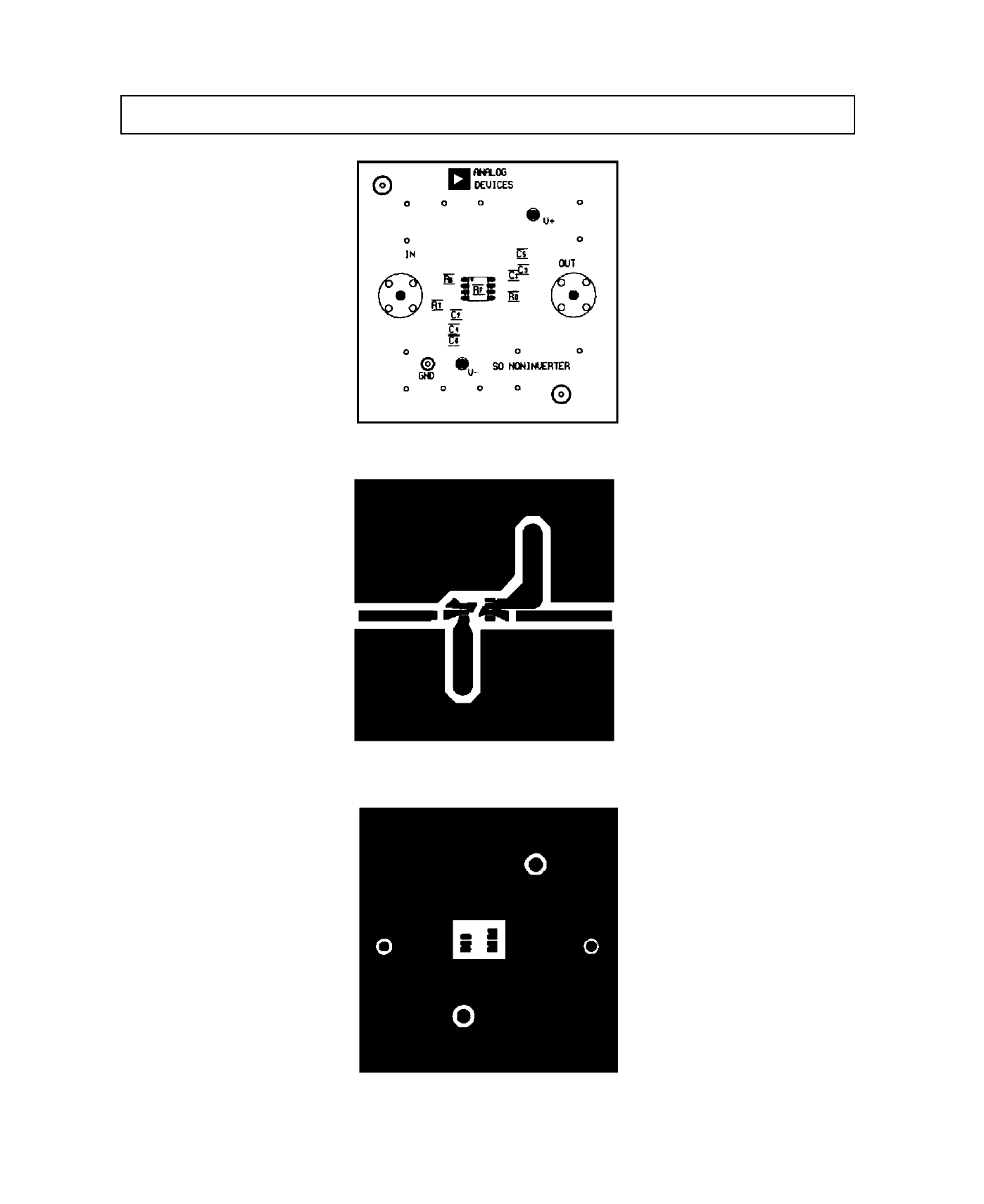
LAYOUT CONSIDERATIONS
The specified high speed performance of the AD8011 requires
careful attention to board layout and component selection.
Table I shows the recommended component values for the
AD8011 and Figures 38–40 show the layout for the AD8011
evaluation board (8-pin SOIC, Gain = +2). Proper R
F
design tech-
niques and low parasitic component selection are mandatory.
The PCB should have a ground plane covering all unused por-
tions of the component side of the board to provide a low im-
pedance ground path. The ground plane should be removed
from the area near the input pins to reduce stray capacitance.
Chip capacitors should be used for supply bypassing (see Fig-
ure 37). One end should be connected to the ground plane
and the other within 1/8 in. of each power pin. An additional
(4.7
µ
F–10
µ
F) tantalum electrolytic capacitor should be con-
nected in parallel.
The feedback resistor should be located close to the inverting
input pin in order to keep the stray capacitance at this node to a
minimum. Capacitance greater than 1.5 pF at the inverting in-
put will significantly affect high speed performance when oper-
ating at low noninverting gains.
Stripline design techniques should be used for long signal traces
(greater than about 1 in.). These should be designed with the
proper system characteristic impedance and be properly termi-
nated at each end.
C1
0.01µF
C2
0.01µF
C4
10µF
C3
10µF
R
T
INVERTING CONFIGURATION
V
IN
V
OUT
+V
S
–V
S
R
G
R
F
R
O
C1
0.01µF
C2
0.01µF
C4
10µF
C3
10µF
R
T
NONINVERTING CONFIGURATION
V
IN
V
OUT
+V
S
–V
S
R
G
R
F
R
O
Figure 37. Inverting and Noninverting Configurations
Table I. Typical Bandwidth vs. Gain Setting Resistors
Small Signal –3 dB BW
Gain
R
F
R
G
R
T
(MHz), V
S
=
±
5 V
–1
1000
Ω
1000
Ω
52.3
Ω
150
–2
1000
Ω
499
Ω
54.9
Ω
130
–10
499
Ω
49.9
Ω
–
140
+1
1000
Ω
–
49.9
Ω
400
+2
1000
Ω
1000
Ω
49.9
Ω
250
+10
422
Ω
47.5
Ω
49.9
Ω
100
+6
1000
Ω
200
Ω
49.9
Ω
70
+6
500
Ω
100
Ω
49.9
Ω
170
R
T
chosen for 50
Ω
characteristic input impedance.
R
O
chosen for characteristic output impedance.
AD8011
REV. 0
–15–
Figure 39. Evaluation Board Layout (Solder Side)
Figure 38. Evaluation Board Silkscreen (Top)
Figure 40. Evaluation Board Layout (Component Side)
REV. 0
–16–
AD8011
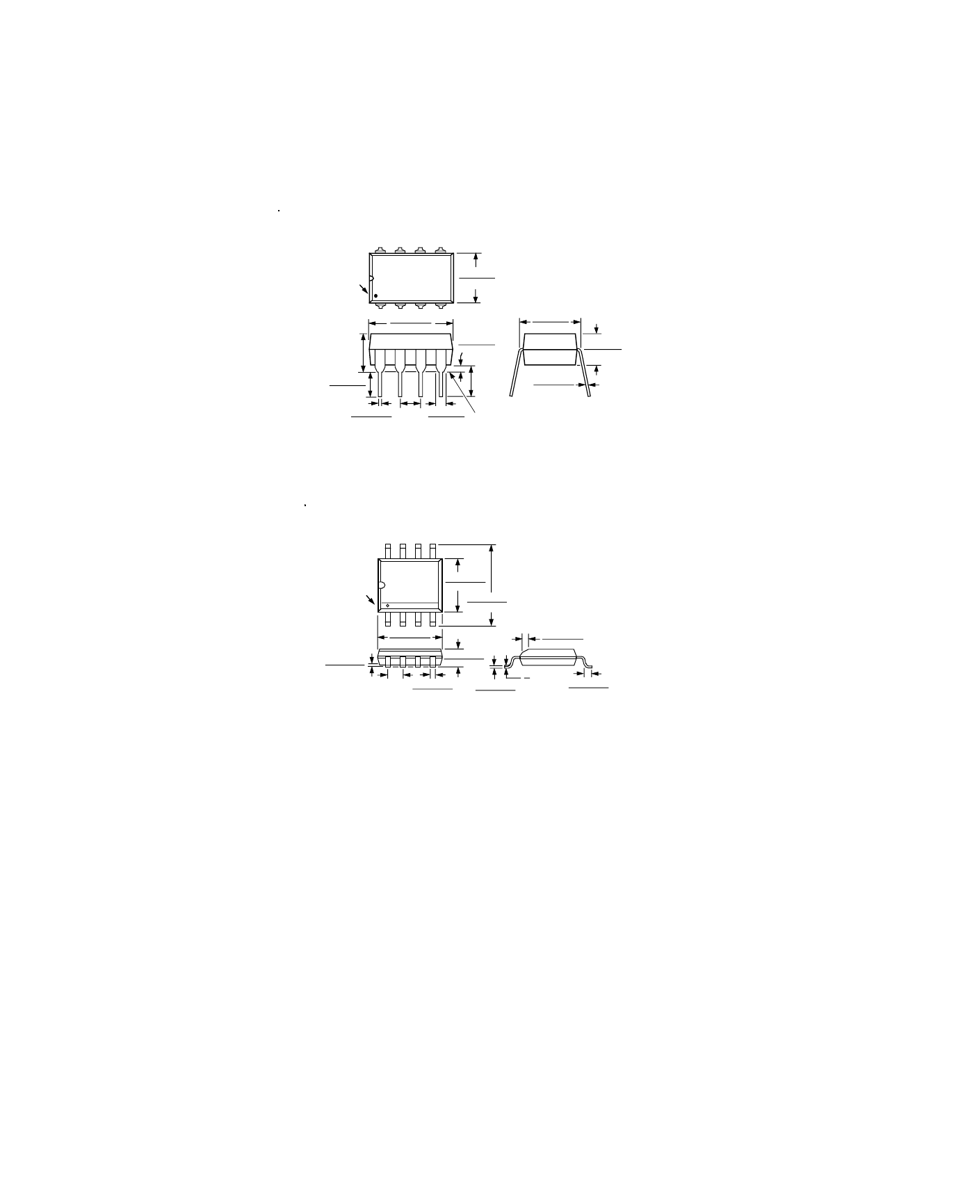
OUTLINE DIMENSIONS
Dimensions shown in inches and (mm).
8-Pin Plastic DIP
(N Package)
8-Pin Plastic SOIC
(R Package)
PIN 1
0.1574 (4.00)
0.1497 (3.80)
0.2440 (6.20)
0.2284 (5.80)
4
5
1
8
0.0098 (0.25)
0.0075 (0.19)
0.0500 (1.27)
0.0160 (0.41)
8
°
0
°
0.0196 (0.50)
0.0099 (0.25)
x 45
°
0.0500
(1.27)
BSC
0.0688 (1.75)
0.0532 (1.35)
0.0098 (0.25)
0.0040 (0.10)
0.1968 (5.00)
0.1890 (4.80)
0.0192 (0.49)
0.0138 (0.35)
PIN 1
0.280 (7.11)
0.240 (6.10)
4
5
8
1
0.060 (1.52)
0.015 (0.38)
0.130
(3.30)
MIN
0.210
(5.33)
MAX
0.160 (4.06)
0.115 (2.93)
0.430 (10.92)
0.348 (8.84)
SEATING
PLANE
0.022 (0.558)
0.014 (0.356)
0.070 (1.77)
0.045 (1.15)
0.100
(2.54)
BSC
0.325 (8.25)
0.300 (7.62)
0.015 (0.381)
0.008 (0.204)
0.195 (4.95)
0.115 (2.93)
C2002–7.5–2/95
PRINTED IN U.S.A.