
One Technology Way, P.O. Box 9106, Norwood. MA 02062-9106, U.S.A.
Tel: 617/329-4700
Fax: 617/326-8703
a
Evaluation Board for
Loop Powered 4-20mA DAC
EVAL-AD421EB
FEATURES
Loop Powered
5V, 3.3V and 3V Modes of Operation
Direct Hook-Up to Printer Port of PC
PC Software for Control of Loop Current
Included on the evaluation board, along with the AD421, are a
DN2535/DN2540, an N-Channel depletion mode FET which is
used as part of the regulator loop to regulate the supply for the
board from the externally supplied loop voltage applied between
the loop(+) and loop (-) inputs, digital buffers to buffer and
level shift the input signals from the printer port edge connector
and a number of passive components required to achieve
optimum performance from the AD421.
Interfacing to the AD421 board is provided via a 36-Pin
Centronics Connector.
OPERATING THE AD421 EVALUATION BOARD
Power Supplies
The evaluation board operates from a single power supply
connected between the LOOP PLUS and LOOP MINUS
terminals on the board. This loop power supply must be floating
with respect to the computer ground and have a minimum limit
of V
CC
+2 V and a maximum limit of the breakdown voltage of
the external pass transistor. The pass transistor used on this
board is a DN2535/DN2540, N-Channel Depletion mode
transistor available from Supertex inc.., this facilitates the use of
loop voltages up to 350V. This pass transistor in association
with the regulator loop of the AD421 regulates the supply
voltage for the AD421 itself and for the digital buffers on the
board. The regulated voltage is referenced to the COM pin on
the AD421. A link option on the board selects the operating
mode for the board to be either 5V, 3.3V or 3V.
The regulated voltage on the AD421 V
CC
pin is decoupled with
10
µ
F tantalum and 0.1
µ
F ceramic disc capacitors.
The loop current can be measured in either the LOOP PLUS or
LOOP MINUS lines.
INTRODUCTION
This Application Note describes the evaluation board for the
AD421, loop powered 4-20mA DAC. The AD421 is a
complete, loop-powered, digital to 4-20mA converter, designed
to meet the needs of smart transmitter manufacturers in the
Industrial Control industry. It provides a high precision, fully
integrated, low cost solution in a compact 16-pin package. The
AD421 is ideal for extending the resolution of smart 4-20mA
transmitters at very low cost.
The AD421 includes a selectable regulator which can be used to
power all other devices in the transmitter. This regulator
provides either a +5 V, +3.3 V or +3 V regulated output
voltage. The part also contains +1.25 V and +2.5 V precision
references. The AD421 thus eliminates the need for a discrete
regulator and voltage reference. The only external components
required are a number of passive components and a pass
transistor to span large loop voltages. Full data on the AD421 is
available in the AD421 data sheet available from Analog
Devices and should be consulted in conjunction with this
Application Note when using the Evaluation Board.
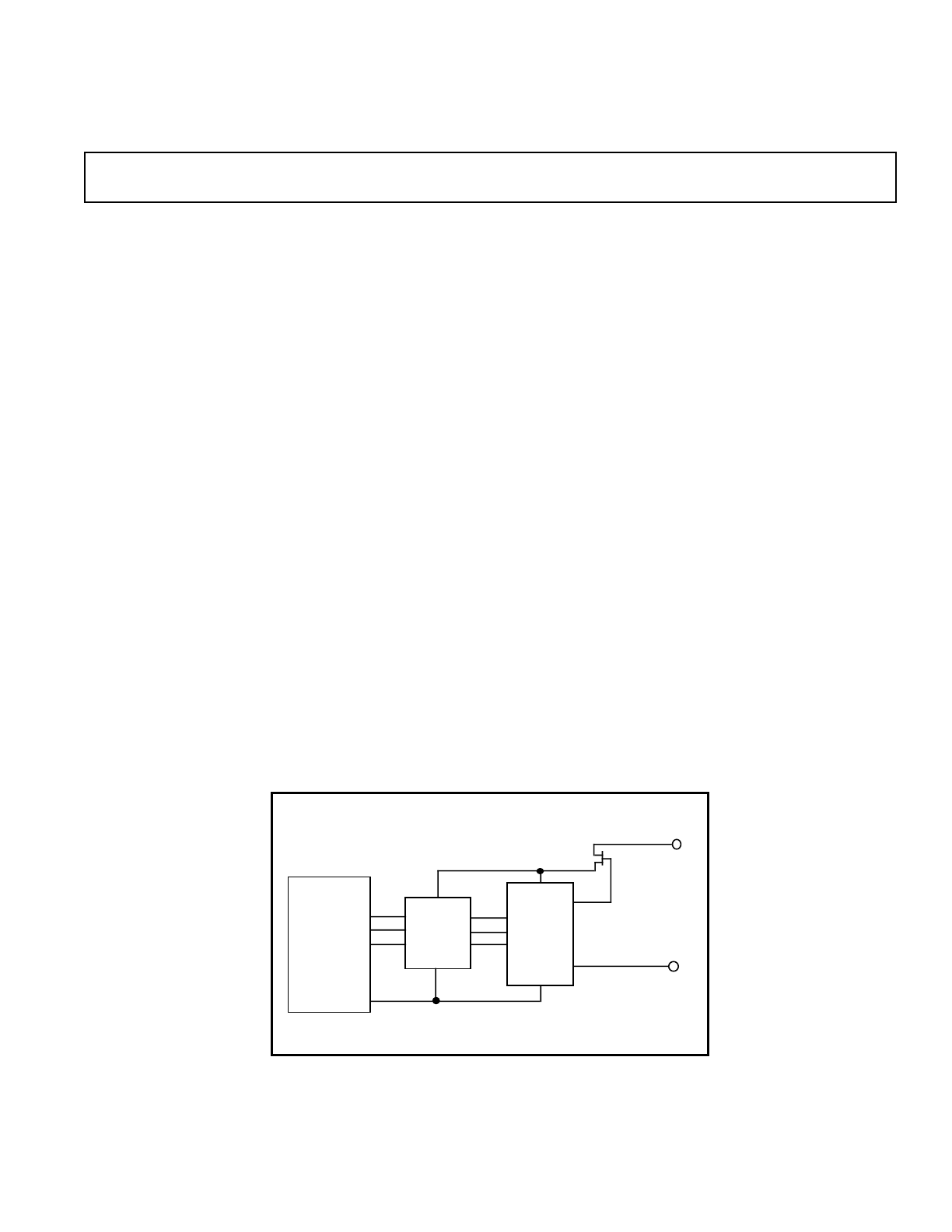
FUNCTIONAL BLOCK DIAGRAM
36-WAY
CENTRONICS
CONNECTOR
LEVEL
SHIFTERS/
BUFFERS
AD421
V
CC
V
CC
COM
DRIVE
LOOP
RTN
DN2535/
DN2540
LOOP
PLUS
LOOP
MINUS
GND
REV. A
Information furnished by Analog Devices is believed to be accurate and
reliable. However, no responsibility is assumed by Analog Devices for its
use, nor for any infringements of patents or other rights of third parties
which may result from its use. No license is granted by implication or
otherwise under any patent or patent rights of Analog Devices.

EVAL-AD421EB
REV. A
–2–
Link Options
There is one link option on the evaluation board which should
be set for the required operating setup before using the board.
The function of this link option is described below.
LK1
Function
This option is used to control the selectable
regulator on the AD421 that is used to power
the AD421 itself and the digital buffers on the
board.
Position
Function
A
With this link in position A, the LV pin on the
AD421 is connected to COM, in this position
the regulated voltage for the AD421 and the
digital buffer is set to 5V.
B
With this link in position B, the LV pin on the
AD421 is connected to V
CC
, in this position the
regulated voltage for the AD421 and the digital
buffer/level shifter is set to 3V.
C
With this link in position C, the LV pin on the
AD421 is connected through a 0.01uF capacitor
to V
CC
, in this position the regulated voltage for
the AD421 and the digital buffer/level shifter is
set to 3.3V.
EVALUATION BOARD INTERFACING
Interfacing to the evaluation board is via a 36-pin Centronics
connector, SKT1 using a standard parallel printer port cable.
The pinout for the SKT1 connector is given in Figure 1 and its
corresponding pin designations are given in Table I. The
evaluation board should be powered up before a cable is
connected to the connector.
The digital interface on the AD421 consists of just three wires:
DATA, CLOCK and LATCH. The interface connects directly
to the serial ports of commonly-used microcontrollers without
the need for any external glue logic. On this evaluation board
the PC via the printer port is used to emulate a microcontroller.
Data is loaded MSB first into the input shift register of the
AD421 on the rising edge of the CLOCK signal and is trans-
ferred to the DAC latch on the rising edge of the LATCH
signal. This data can take two forms; normal 4-20mA data and
alarm current data. The first form is where the AD421 operates
over its normal 4mA to 20mA output range with 16-bits of
resolution between these end-points. The second form allows
the user to program a current value outside this range as an
indication from the transmitter than there is a problem with the
transducer i.e. tranducer burnout. The AD421 counts the
number of clock pulses which it receives between LATCH
signals as a means of determining whether the data clocked in is
4-20mA data or alarm current data.
If there are 16 rising clock edges between successive LATCH
pulses then the data to be loaded to the input shift register is
assumed to be normal 4-20mA data.
If there are more than 16 rising clock pulses between successive
LATCH pulses then the data to be loaded to the input shift
register is assumed to be alarm current data.
Table I. SKT1 Pin Designations
1
NC
No Connect. This pin is not connected
on the evaluation board.
2
NC
No Connect. This pin is not connected
on the evaluation board.
3
LATCH
Latch Input. The signal on this pin is
buffered in 5V operating mode and
level translated in both 3.3V and 3V
modes using a 74HC4050 before being
applied to the LATCH pin of the
AD421. On the rising edge of the latch
signal
data is loaded from the input
register to the DAC register and the
DAC output is updated.
4
NC
No Connect. This pin is not connected
on the evaluation board.
5
CLOCK
Serial Clock. The signal on this pin is
buffered when using a V
CC
of 5V and
level translated when V
CC
is 3.3V or 3V
before being applied to the CLOCK
pin of the AD421. Data on the DATA
pin is clocked into the AD421 shift reg-
ister on the rising edge of this clock in-
put.
6-8
NC
No Connect. These pins are not con-
nected on the evaluation board.
9
DATA
Serial Data Input. Data applied to this
pin is buffered when using a V
CC
of 5V
and level translated when V
CC
is 3.3V
or 3V before being applied to the
AD421's DATA pin. The serial data
applied to the DATA pin is written to
the input shift register on the part. Data
from this input shift register is trans-
ferred to the data register on the rising
edge of the LATCH signal.
10-18
NC
No Connect. These pins are not con-
nected on the evaluation board.
19-25
DGND
Ground reference point for digital input
signals. Connects to the COM plane on
the evaluation board.
26-36
NC
No Connect. These pins are not con-
nected on the evaluation board.
Figure 1. SKT1 Pin Configuration, Pin View.
1
18
19
36
EVAL-AD421EB
REV. A
–3–
RUNNING THE AD421 INTERFACE SOFTWARE
Included in the evaluation board package is a PC-compatible
disk which contains software for controlling and evaluating the
performance of the AD421 using the printer port of a PC. There
are a total of thirteen files on the distribution disk.
To use the software, the user must have an IBM-compatible PC
and Windows 3.1 must be installed. Start Windows and, using
either the RUN command or the file manager, start the program
called SETUP.EXE on the distribution disk. This automatically
installs the application and sets up a window called ANALOG
DEVICES. The application ICON is found here. To start the
application, double click on the ICON.
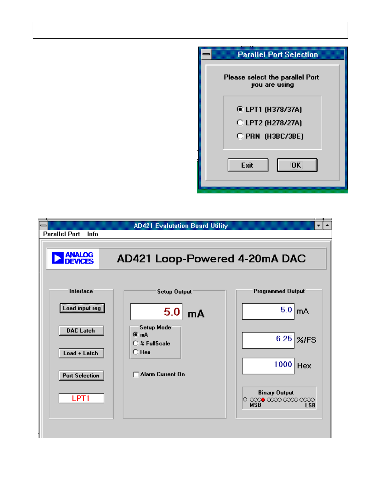
PRINTER PORT SELECTION
When the program starts, a window as shown in Figure 2
appears and the user is asked to select a printer port. The user
can select the port they wish to use by cliciking on the appropri-
ate option button and then clicking OK. The hexadecimal
numbers displayed beside each option correspond to the
memory address of the port in question. The correct selection
depends on what type of computer is being used (Desktop,
Laptop etc). LPT1 works for most machines and is the default
selection. When using a Compaq laptop, select PRN. A
different port can be selected at any time from the MAIN
MENU.
Figure 2. Parallel Port Selection.
Figure 3. Main Window.

EVAL-AD421EB
REV. A
–4–
The evaluation software does not allow another application
running under Windows to access the printer port while it is
running. Control of the printer port is returned when the
AD421 application program is quit.
MAIN MENU WINDOW
Once the OK button of the port selection window has been
pressed the user is presented with the Main Menu Window for
the application. The window is called AD421 Evaluation Board
Utility and is as shown in Figure 3. This utility contains the
following sections: interface, setup output and programmed
output.
INTERFACE SECTION
The interface section contains buttons that control the method
in which data is loaded to the AD421 and also the printer port
selection. The following is a description of these buttons.
Load Input Reg
When this button is clicked the input register of the AD421 is
loaded with the data as programmed in the Setup Output
section. Data is only loaded to the input register and is not
transferred to the DAC register. No output update takes place
in this case.
DAC Latch
When this button is clicked the data in the input register of the
AD421 is transferred to the DAC register and an output update
takes place. This basically activates the LATCH input to the
AD421.
Load + Latch
When this button is clicked the input register of the AD421 is
loaded with the data as programmed in the Setup Output
Section and the LATCH signal is also activated updating the
output of the AD421. This is a combination of the previous two
buttons.
Port Selection
This button returns the user to the previous menu on Parallel
Port Selection. The selected port appears in the box at the
bottom on the interface section.
SETUP OUTPUT SECTION
This section allows the user to select one of three current output
setup modes and also allows the selection of either 4-20mA
normal mode of operation or the selection of an alarm current
mode where the current range is from 3.5-24mA. The following
is a description of these buttons.
Setup Mode
There are three selections in this setup, the programmed output
current can be programmed as a straight mA by selecting the
mA button.
The second button, % Fullscale, allows the output current to be
programmed as a percentage of the fullscale output.
The third selection allows the user to enter the HEX data value
to be loaded to the input register as the method of programming
the output current.
Alarm Current On
This button is used to select between the normal 4-20mA
output and the alarm current output. When this button is not
selected the normal 4-20mA output range is selected. When the
alarm current on is selected an "x" appears in the box and the
output range can be programmed from 3.5mA to 24mA.
PROGRAMMED OUTPUT
This section shows the programmed output current as a current
in mA, as a % of Fullscale and as the HEX value that has been
written to the input register. The Binary Output Box shows in
the form of a LED display the data that has been loaded to the
AD421.
EVAL-AD421EB
REV. A
–5–
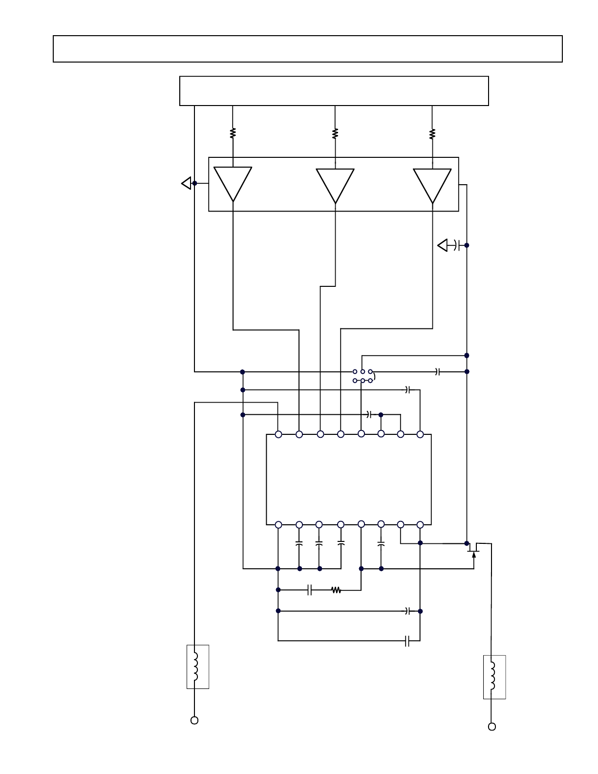
Figure 4. AD421 Evaluation Board Circuit Diagram.
VCC
DGND
1/2 74HC4050
REF OUT1
REF OUT2
REF IN
LV
LATCH
CLOCK
DATA
LOOP RTN
VCC
BOOST
COMP
DRIVE
C1
C2
C3
COM
AD421
C3
0.0033
µ
F
C2
0.01
µ
F
C1
0.01
µ
F
C6
0.01
µ
F
C5
4.7
µ
F
C4
4.7
µ
F
LOOP PLUS
LOOP MINUS
CENTRONICS
CONNECTOR
P1_3
P1_5
P1_9
P1_18-25
LK 1
DN2535/
DN2540
C7
10
µ
F
C8
0.1
µ
F
1000pF
1k
Ω
28F0195 - 100
28F0195 - 100
A
B
C
0.01
µ
F
10 k
Ω
10 k
Ω
10 k
Ω
R1
R2
R3
R4
0.1
µ
F
C9
C10
C11
U3
P1
U1
U2
P2
P2
EMI Supression
Component
EMI Supression
Component
L2
L1

EVAL-AD421EB
REV. A
–6–
COMPONENT LISTING AND MANUFACTURERS
Intergrated Circuits
Component
Location
Vendor
AD421
U1
Analog Devices
DN2535/DN2540
U2
Supertex
1
74HC4050
U3
Philips
Capacitors
Component
Location
Vendor
0.01
µ
F Ceramic
C1, C2
Philips
Mftrs No. CW20C 103M
0.0033
µ
F Ceramic
C3
4.7
µ
F
±
20% Tantalum (16 V)
C4, C5
AVX- Kyocera
Mftrs No TAG106MO16
0.01
µ
F Ceramic(X7R
±
20%)
C6, C10
Philips
Mftrs No. CW20C 103M
10
µ
F
±
20% Tantalum (16 V)
C7
AVX- Kyocera
Mftrs No TAG106MO16
0.1
µ
F Ceramic(X7R
±
20%)
C8, C11
Philips
Mftrs No. CW20C 104M
1000pF Ceramic
C9
Philips
Mftrs No. CW15A102M
Resistors
Component
Location
Vendor
1k
Ω
±
5% 0.25W
Carbon Film Resistor
R1
Bourns
10k
Ω
±
5% 0.25W
Carbon Film Resistor
R2, R3, R4
Bourns
EMI/EMC Ferrites
Component
Location
Vendor
28F0195-100
Ferrites
L1,L2
Steward
2
Link Options
Component
Location
Vendor
Pin Headers
Lk1 (3x2 way)
Harwin
Mftrs No. M20-9993606
Shorting Plugs
Pin Headers
Harwin
(1 required)
Mftrs No. M7571-05
Sockets
Component
Location
Vendor
36 Pin Centronics Connector
P1
Fujitsu
Mftrs No. FCN785J036G0
16-Pin IC Socket
U1,U2
Harwin
Mftrs No. D2816-01
PCB Mounting Terminal Block
P2 (LOOP PLUS,
Lumberg
LOOP MINUS)
Mftrs No. KRM2
1
Supertex inc., 1350 Bordeaux Drive, Sunnyvale, California 94089. Tel No. 408 744 0100
2
Steward, 1200 East 36th Street, P.O. Box 510, Chattanooga, Tennessee 37401-0510. Tel No. 423 867 4100.

EVAL-AD421EB
REV. A
–7–
EMI/EMC CONSIDERATIONS
On the AD421 board care was taken with the layout, grounding
and decoupling to reduce any effects that electromagnetic
disturbances might have on the AD421. Two ferrites, L1 and L2
are included on the AD421 board to provide an extra level of
security against EMI disturbances that come in on the loop(+)
and loop(-) lines. EMC susceptibility tests were carried out on
the AD421 board to check the level of performance obtained
from this board when subjected to various electromagnetic
disturbances. The aim of the susceptibility tests is to ensure that
the product has an adequate level of intrinsic immunity to
electromagnetic disturbance to enable it to operate as intended.
The EMI/EMC directive 89/336/EEC only applies to products
or systems and not to individual components. The AD421
evaluation board acts as a system in this test procedure. The
immunity tests performed included conducted immunity and
radiated immunity. Conducted immunity is a fast transient burst
test where fast transients are coupled onto the 4-20ma loop
twisted pair cable using a 1m capacitive clamp. Radiated
immunity testing involves subjecting the board under test to
various electric fields with frequencies varying from 30MHz to
1GHz.
Radiated Immunity (IEC 1000-4-3)
This set of experiments looked at the performance of the AD421
when subjected to various electric fields. Class B approval for
use in residential/commercial light industrial environments
requires the system to remain functional in a field of 3V/m from
30MHz to 1GHZ. Class A approval for use in industrial
environments requires the system to remain functional in a field
of 10V/m. This test is carried out in a stripline cell which is
essentially two metal plates placed in parallel, the AD421 board
is placed between these plates where it is subjected to an electric
field applied to the plates. The results obtained from this test
with the AD421 in its normal operating mode with Vcc =5V and
controlling the current in the loop to 10mA are as follows.
Board in Horizontal Orientation:
Field Strength Results Comments
3V/m
PASS
Range from 30MHz to 1GHz
5V/m
PASS
Range from 30MHz to 1GHz
10V/m
PASS
Range from 30MHz to 1GHz
This is class 1 performance, i.e. normal operation maintained
during application on the field.
Board in Vertical Orientation:
Field Strength Results Comments.
3V/m
PASS
Range from 30MHz to 1GHz
5V/m
PASS
Range from 30MHz to 1GHz
10V/m
FAIL
Device resets to 4mA at 860MHz
This is class 1 performance, ie normal operation maintained
during application of the fields of 3V/m and 5V/m. The classifi-
cation is class 3 at 10V/m as user intervention is required to get
the AD421 back to its programmed conditions.
Conducted Immunity (IEC 1000-4-4 Fast Transient Burst
Test)
This set of experiments involved the coupling of fast transients
onto the current loop unshielded twisted pair cable through a
1m capacitive clamp. The fast transient burst is specified to
have a rise time of 5ns and a duration of 50ns and is supplied
from a 50
Ω
source. Bursts of 15ms duration of these pulses at a
repetition rate of 5kHz are applied every 300ms. The voltage
level of the pulse is controlled from 250V to 5kV. Coupling onto
the cable is via a capacitive clamp which is essentially two metal
plates which sandwich the line under test to provide a distrib-
uted coupling capacitance. This clamp is fed from the transient
generator which is constructed with a spark gap driven from an
energy storage capacitor which enables the high voltages to be
generated with the fast rise times. The AD421 is programmed
so that 10mA flows in the loop during the experiments. The
results from this test were as follows:
Burst Amplitude Results
Comments.
500V Positive
PASS
Normal Operation.
500V Negative
PASS
Normal Operation.
1kV Positive
FAILS
Loop current resets to 4mA.
1kV Negative
FAILS
Loop current resets to 4mA.
2kV Positive
FAILS
Loop current resets to 4mA.
2kV Negative
FAILS
Loop current goes to 20mA.
The board achieves class 1 performance for application of a
burst of 500V, ie it continues to work as normal. For all other
bursts the operation can be classified as class 3 where user
intervention is required to restore the part back to normal
operation after the burst has been removed.
Further development work on the AD421 evaluation board is
being planned to see if the above performance can be improved
upon.