
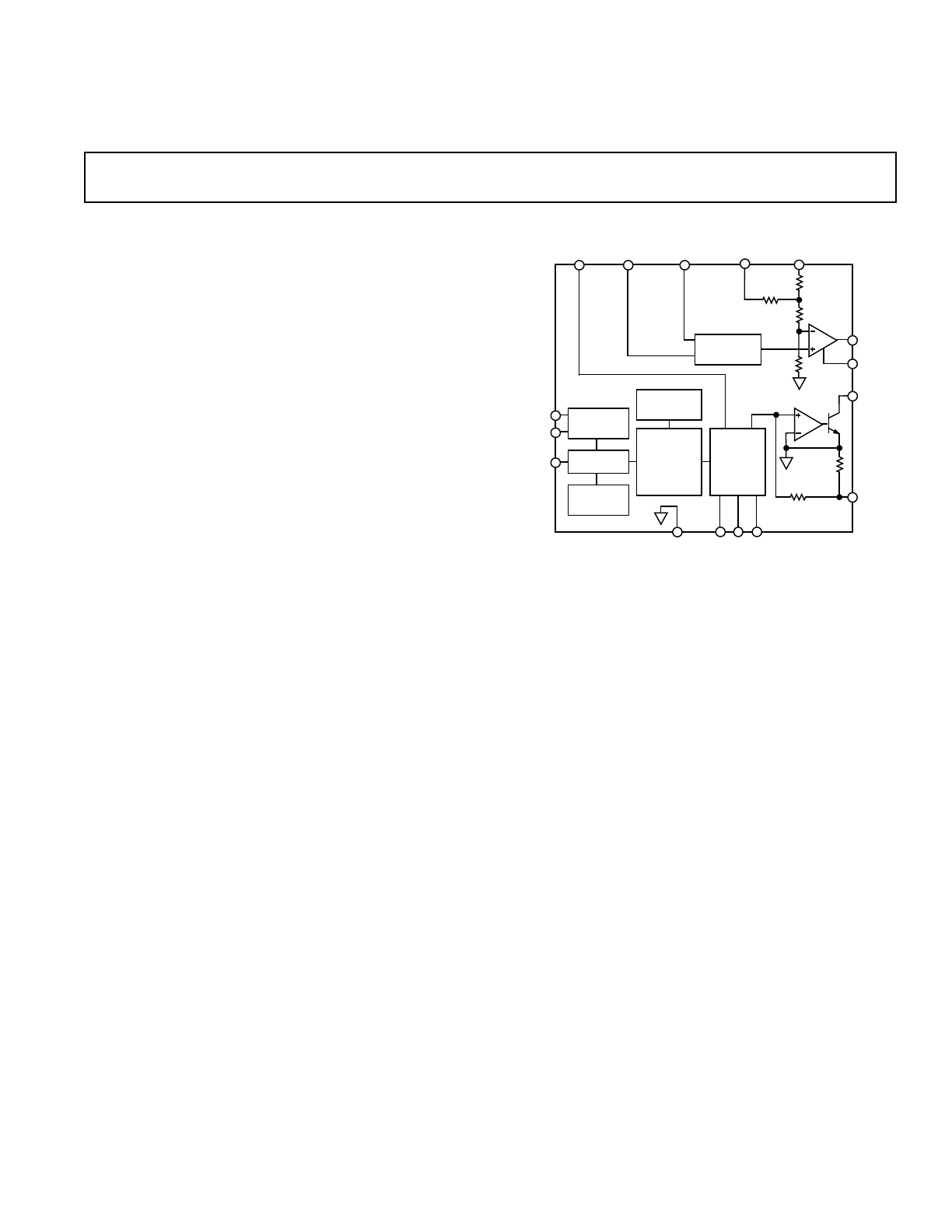
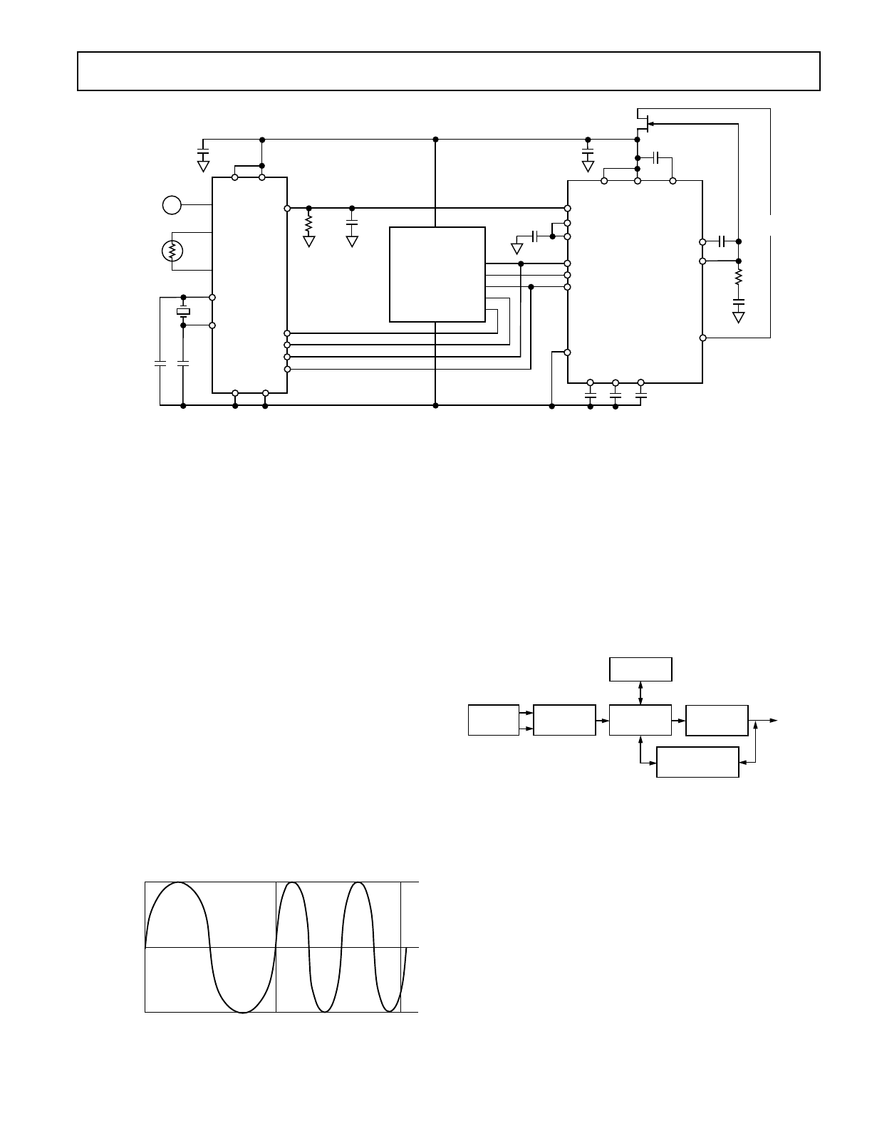
FUNCTIONAL BLOCK DIAGRAM
REV. 0
Information furnished by Analog Devices is believed to be accurate and
reliable. However, no responsibility is assumed by Analog Devices for its
use, nor for any infringements of patents or other rights of third parties
which may result from its use. No license is granted by implication or
otherwise under any patent or patent rights of Analog Devices.
a
FEATURES
4–20 mA Current Output
HART* Compatible
16-Bit Resolution and Monotonicity
60.01% Integral Nonlinearity
5 V or 3 V Regulator Output
2.5 V and 1.25 V Precision Reference
750
mA Quiescent Current max
Programmable Alarm Current Capability
Flexible High Speed Serial Interface
16-Pin TSSOP, SOIC and PDIP Packages
Loop-Powered
4–20 mA DAC
© Analog Devices, Inc., 1996
One Technology Way, P.O. Box 9106, Norwood, MA 02062-9106, U.S.A.
Tel: 617/329-4700
Fax: 617/326-8703
AD421
PRODUCT HIGHLIGHTS
1. The AD421 is a single chip, high performance, low cost
solution for generating 4–20 mA signals for smart industrial
control transmitters.
2. The AD421’s regulated supply voltage can be used to power
any additional circuits in the transmitter. The regulated
output value is pin selectable as either +3 V, +3.3 V or +5 V.
3. The AD421’s on-chip references can provide a precision
reference voltage to other devices in the system. This
reference voltage can be either +1.25 V or +2.5 V.
4. The AD421 is fully compatible with standard HART
circuitry or other similar FSK protocols.
5. With the addition of a single discrete transistor, the AD421
can be operated from V
CC
+ 2 V min to a maximum of the
breakdown voltage of the pass transistor.
6. The AD421 converts the digital data to current with 16-bit
resolution and monotonicity. Full-scale settling time to
±
0.1% typically occurs within 8 ms.
7. The AD421 features a programmable alarm current capabil-
ity that allows the transmitter to send out of range currents to
indicate a transducer fault.
*HART is a trademark of the HART Communication Foundation.
†Index on Page 14.
GENERAL DESCRIPTION
The AD421 is a complete, loop-powered, digital to 4–20 mA
converter, designed to meet the needs of smart transmitter
manufacturers in the Industrial Control industry. It provides a
high precision, fully integrated, low cost solution in a compact
16-pin package. The AD421 is ideal for extending the resolution
of smart 4–20 mA transmitters at very low cost.
The AD421 includes a selectable regulator that is used to power
itself and other devices in the transmitter. This regulator
provides either a +5 V, +3.3 V or +3 V regulated output
voltage. The part also contains +1.25 V and +2.5 V precision
references. The AD421 thus eliminates the need for a discrete
regulator and voltage reference. The only external components
required are a number of passive components and a pass
transistor to span large loop voltages.
The AD421 can be used with standard HART FSK protocol
communication circuitry without any degradation in specified
performance. The high speed serial interface is capable of
operating at 10 Mbps and allows for simple connection to
commonly-used microprocessors and microcontrollers via a
standard three-wire serial interface.
The sigma-delta architecture of the DAC guarantees 16-bit
monotonicity while the integral nonlinearity for the AD421 is
±
0.01%. The part provides a zero scale 4 mA output current
with
±
0.1% offset error and a 20 mA full-scale output current
with
±
0.2% gain error.
The AD421 is available in a 16-pin, 0.3 inch-wide, plastic DIP,
a 16-lead, 0.3 inch-wide, SOIC package and in a 16-lead TSSOP
package. The part is specified over the industrial temperature
range of –40
°
C to +85
°
C.
INPUT SHIFT
REGISTER
DAC LATCH
POWER-ON
RESET
LOCAL
OSCILLATOR
SWITCHED
CURRENT
SOURCES
AND
FILTERING
BANDGAP
REFERENCE
REF IN
(+2.5V)
REF OUT1
(+1.25V)
REF OUT2
(+2.5V)
LV
V
CC
DRIVE
COMP
BOOST
LOOP
RTN
C1 C2 C3
COM
LATCH
CLOCK
DATA
40
Ω
16-BIT
SIGMA-
DELTA DAC
75k
Ω
112.5k
Ω
134k
Ω
121k
Ω
80k
Ω
AD421

AD421–DAC SPECIFICATIONS
Parameter
B Versions
2
Units
Conditions/Comments
ACCURACY
Resolution
16
Bits
Monotonicity
16
Bits min
Integral Nonlinearity
±
0.01
% of FS max
FS = Full-Scale Output Current
Offset (4 mA) @ +25
°
C
4
±
0.1
% of FS max
V
CC
= 5 V
Offset Drift
±
25
ppm of FS/
°
C max
Includes On-Chip Reference Drift
Total Output Error (20 mA) @ +25
°
C
4
±
0.2
% of FS max
V
CC
= 5 V
Total Output Drift
±
50
ppm of FS/
°
C max
Includes On-Chip Reference Drift
V
CC
Supply Sensitivity
50
nA/mV max
25 nA/mV Typical
VOLTAGE REFERENCE
REF OUT2
Output Voltage
2.49/2.51
V min/V max
2.5 V Nominal
Drift
±
40
ppm/
°
C max
20 ppm/
°
C Typical from –40
°
C to +25
°
C and
–2.5 ppm/
°
C Typical from +25
°
C to +85
°
C
Externally Available Current
0.5
mA min
V
CC
Supply Sensitivity
150
µ
V/V max
15
µ
V/V Typical
Output Impedance
3
Ω
typ
Noise (0.1 Hz – 10 Hz)
6
µ
V (p-p) typ
REF OUT1
Output Voltage
1.24/1.26
V min/V max
1.25 V Nominal, 100 k
Ω
Load to COM
5
Drift
±
50
ppm/
°
C max
20 ppm/
°
C Typical from –40
°
C to +25
°
C and
2 ppm/
°
C Typical from +25
°
C to +85
°
C
Externally Available Current
0.5
mA min
V
CC
Supply Sensitivity
150
µ
V/V max
15
µ
V/V Typical
Output Impedance
3
Ω
typ
Noise (0.1 Hz – 10 Hz)
4
µ
V (p-p) typ
REF IN
Input Resistance
40
k
Ω
typ
DIGITAL INPUTS
V
IH
(Logic 1)
0.75
×
V
CC
V min
V
IL
(Logic 0)
0.25
×
V
CC
V max
I
IH
±
10
µ
A max
V
IN
= V
CC
I
IL
±
10
µ
A max
V
IN
= 0 V
Data Coding
Binary
Data Rate
10
Mbps max
POWER SUPPLIES
Operating Range
+2.95 to +5.05
V min to V max
Functional to 7 V
Quiescent Current
@ V
CC
= 3 V
650
µ
A max
475
µ
A Typical
@ V
CC
= 5 V
750
µ
A max
575
µ
A Typical
NOTES
1
The DN25D is available from Supertex, Inc., 1350 Bordeaux Drive, Sunnyvale, CA 94089.
2
Temperature range is –40
°
C to +85
°
C.
3
The max current loop voltage compliance is determined by the pass transistor breakdown voltage and is 350 V for the DN25D.
4
With V
CC
= 3 V, the transfer function shifts negative by typically 0.25%; a 16 k
Ω
resistor connected between COM and LOOPRTN will approximately compensate
for the V
CC
supply sensitivity in moving from 5 V to 3 V by skewing the gain of the AD421.
5
100 k
Ω
resistor only required if this reference is being used in application circuits.
Specifications subject to change without notice.
AD421–LOOP-POWERED SPECIFICATIONS
Parameter
B Versions
2
Units
Conditions/Comments
OUTPUT CHARACTERISTICS
Current Loop Voltage Compliance
3
V
CC
+ 2
V min
350
V max
DN25D Breakdown Voltage
Full-Scale Settling Time
8
ms typ
Settling Time to
±
0.1%, C1 = C2 = 10 nF, C3 = 3.3 nF
Output Impedance
25
M
Ω
typ
AC Loop Voltage Sensitivity
2
µ
A/V typ
1200 Hz to 2200 Hz
VOLTAGE REGULATOR
Output Voltage (V
CC
)
3 V Mode
2.95/3.05
V min/V max
3 V Nominal. LV Pin Connected to V
CC
3.3 V Mode
3.25/3.35
V min/V max
3.3 V Nominal. LV Pin Connected Through 0.01
µ
F to V
CC
5 V Mode
4.95/5.05
V min/V max
5 V Nominal. LV Pin Connected to COM
Externally Available Current
3.25
mA min
Assuming 4 mA Flowing in the Loop
Line Regulation
1
µ
V/V typ
Load Regulation
15
µ
V/mA typ
–2–
(Using DN25D
1
as pass transistor as per Figure 3;
REF IN = REF OUT2; T
A
= T
MIN
to T
MAX
unless otherwise noted)
REV. 0
(V
CC
= +3 V to +5 V; REF IN = REF OUT2; T
A
= T
MIN
to T
MAX
unless otherwise noted)
AD421
–3–
REV. 0
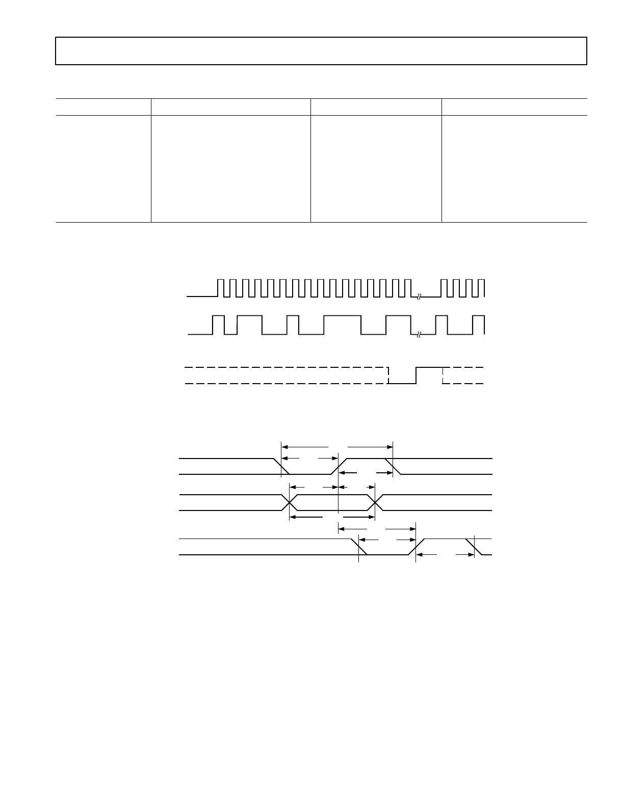
TIMING CHARACTERISTICS
1, 2, 3
Parameter
(B Versions)
Units
Conditions/Comments
t
CK
100
ns min
Data Clock Period
t
CL
50
ns min
Data Clock Low Time
t
CH
50
ns min
Data Clock High Time
t
DW
30
ns min
Data Stable Width
t
DS
30
ns min
Data Setup Time
t
DH
0
ns min
Data Hold Time
t
LD
50
ns min
Latch Delay Time
t
LL
50
ns min
Latch Low Time
t
LH
50
ns min
Latch High Time
NOTES
1
Guaranteed by characterization at initial product release, not production tested.
2
See Figures 1 and 2.
3
All input signals are specified with tr = tf = 5 ns (10% to 90% of V
CC
) and timed from a voltage level of (V
IN
+ V
IL
)/2; tr and tf should not exceed 1
µ
s on any digital
input.
WORD "N"
WORD "N +1"
1
0
1
1
1
1
1
1
1
1
0
0
0
0
0
0
1
0
0
1
CLOCK
DATA
LATCH
B15
(MSB)
B14
B13
B12
B11
B10
B9
B8
B7
B6
B5
B4
B3
B2
B1
B0
B15
B14
B13
B12
(LSB)
Figure 1. Serial Interface Waveforms (Normal Data Load)
CLOCK
DATA
LATCH
t
C K
t
C L
t
C H
t
D S
t
D H
t
D W
t
L D
t
L L
t
L H
Figure 2. Serial Interface Timing Diagram
(V
CC
= +3 V to +5 V, T
A
= T
MIN
to T
MAX
unless otherwise noted)
AD421
–4–
REV. 0
ORDERING GUIDE
Temperature
Package
Model
Range
Option
1
AD421BN
–40
°
C to +85
°
C
N-16
AD421BR
–40
°
C to +85
°
C
R-16
AD421BRRL
–40
°
C to +85
°
C
R-16; Reeled SOIC
AD421BRURL
–40
°
C to +85
°
C
RU-16; Reeled TSSOP
2
AD421BRURL7
–40
°
C to +85
°
C
RU-16; Reeled TSSOP
3
EVAL-AD421-EB
Evaluation Board
NOTES
1
N = Plastic DIP, R = SOIC, RU = TSSOP.
2
Available on 13" reel; min order quantity is 4,000.
3
Available on 7" reel; min order quantity is 1,400.
ABSOLUTE MAXIMUM RATINGS*
(T
A
= +25
°
C unless otherwise noted)
DRIVE, BOOST, COMP to COM . . . . –0.5 V to V
CC
+ 0.5 V
LOOP RTN to COM . . . . . . . . . . . . . . . . . . . –2 V to + 0.5 V
Digital Input Voltage to COM . . . . . . . . –0.5 V to V
CC
+ 0.5 V
Operating Temperature Range
Commercial (B Version) . . . . . . . . . . . . . . – 40
°
C to +85
°
C
Storage Temperature Range . . . . . . . . . . . . –65
°
C to +150
°
C
Junction Temperature . . . . . . . . . . . . . . . . . . . . . . . . +150
°
C
Plastic DIP Package, Power Dissipation . . . . . . . . . . 670 mW
θ
JA
Thermal Impedance . . . . . . . . . . . . . . . . . . . . 116
°
C/W
Lead Temperature (Soldering, 10 sec) . . . . . . . . . . . . 260
°
C
SOIC Package, Power Dissipation . . . . . . . . . . . . . . . 450 mW
θ
JA
Thermal Impedance . . . . . . . . . . . . . . . . . . . . 110
°
C/W
Lead Temperature, Soldering
Vapor Phase (60 sec) . . . . . . . . . . . . . . . . . . . . . +215
°
C
Infrared (15 sec) . . . . . . . . . . . . . . . . . . . . . . . . . +220
°
C
TSSOP Package, Power Dissipation . . . . . . . . . . . . . 450 mW
θ
JA
Thermal Impedance . . . . . . . . . . . . . . . . . . . . 160
°
C/W
Lead Temperature, Soldering
Vapor Phase (60 sec) . . . . . . . . . . . . . . . . . . . . . +215
°
C
Infrared (15 sec) . . . . . . . . . . . . . . . . . . . . . . . . . +220
°
C
*
Stresses above those listed under “Absolute Maximum Ratings” may cause
permanent damage to the device. This is a stress rating only and functional
operation of the device at these or any other conditions above those listed in the
operational sections of this specification is not implied. Exposure to absolute
maximum rating conditions for extended periods may affect device reliability.
PIN CONFIGURATION
DIP, TSSOP and SOIC
14
13
12
11
16
15
10
9
8
1
2
3
4
7
6
5
TOP VIEW
(Not to Scale)
AD421
REF OUT1
DRIVE
COMP
BOOST
V
CC
REF OUT2
REF IN
LV
C3
C2
C1
LATCH
CLOCK
DATA
LOOP RTN
COM
CAUTION
ESD (electrostatic discharge) sensitive device. Electrostatic charges as high as 4000 V readily
accumulate on the human body and test equipment and can discharge without detection.
Although these devices feature proprietary ESD protection circuitry, permanent damage may
occur on devices subjected to high energy electrostatic discharges. Therefore, proper ESD
precautions are recommended to avoid performance degradation or loss of functionality.
WARNING!
ESD SENSITIVE DEVICE

AD421
–5–
REV. 0
PIN FUNCTION DESCRIPTION
Pin
No.
Mnemonic
Function
1
REF OUT1
Reference Output 1. A precision +1.25 V reference is provided at this pin. It is intended as a precision ref-
erence source for other devices in the transmitter. REF OUT1 is a buffered output capable of providing up
to 0.5 mA to external circuitry.
2
REF OUT2
Reference Output 2. A precision +2.5 V reference is provided at this pin. To operate the AD421 with its
own reference, REF OUT2 should be connected to REF IN. It can also be used as a precision reference
source for other devices in the transmitter. REF OUT2 is a buffered output capable of providing up to
0.5 mA to external circuitry.
3
REF IN
Voltage Reference Input. The reference voltage for the AD421 is applied to this pin and it sets the span for
the AD421. The nominal reference voltage for the AD421 is +2.5 V for correct operation. This can be sup-
plied using an external reference source or by using the part’s own REF OUT2 voltage.
4
LV
Regulated Voltage Control Input. The LV input controls the loop gain of the servo amplifier to set V
CC
. With
LV connected to COM, the regulator voltage is set to 5 V nominal. If the LV input is connected through 0.01
µ
F
to V
CC
, the regulated voltage is nominally 3.3 V. With LV connected to V
CC
the regulated voltage, V
CC
, is 3 V
nominal.
5
LATCH
DAC Latch Input. Logic Input. A rising edge of the LATCH signal loads the data from the serial input shift
register to the DAC latch and hence updates the output of the DAC.
6
CLOCK
Data Clock Input. Data on the DATA input is clocked into the shift register on the rising edge of this
CLOCK input. The period of this clock equals the input serial data bit rate. This serial clock rate can be up
to 10 MHz. If 16 clock cycles are provided between LATCH pulses then the data on the DATA input is
accepted as normal 4–20 mA data. If more than 16 clock cycles are provided between LATCH pulses, the
data is assumed to be alarm current data (see Digital Interface section).
7
DATA
Data Input. The data to be loaded to the AD421 input shift register is applied to this input. Data should be
valid on the rising edge of the CLOCK input.
8
LOOP RTN
Loop Return Output. LOOP RTN is the return path for current flowing in the current loop.
9
COM
Common. This is the reference potential for the AD421 analog and digital inputs and outputs and for the
voltage regulator output.
10
C3
Filtering Capacitor. A low dielectric absorption capacitor ceramic capacitor should be connected between
this pin and COM for internal filtering of the switched current sources.
11
C2
Filtering Capacitor. See C3 description.
12
C1
Filtering Capacitor. See C3 description.
13
DRIVE
Output from the Voltage Regulator Loop. The DRIVE signal controls the external pass transistor to establish and
maintain the correct V
CC
level programmed by the LV inputs while providing the necessary bias as the loop
current is programmed from 4 mA to 20 mA.
14
COMP
Compensation Capacitor Input. A capacitor connected between COMP and DRIVE is required to stabilize
the feedback loop formed with the regulator op amp and the external pass transistor.
15
BOOST
This open collector pin sinks the necessary current from the loop so that the current flowing into BOOST
plus the current flowing into COM is equal to the programmed loop current.
16
V
CC
Power Supply. V
CC
is the power supply input of the AD421 and it also provides the voltage regulator output,
driven by the external pass transistor. It is used both to bias the AD421 itself and to provide power for the
rest of the smart transmitter circuitry. The LV input determines the regulated voltage output to be either
3 V, 3.3 V or 5 V nominal. Alternatively, a separate power supply can be connected to this pin to power the
AD421.
AD421
–6–
REV. 0
Table I. FET Characteristics
FET Type
N-Channel Depletion Mode
I
DSS
24 mA min
BV
DS
(V
LOOP
– V
CC
) min
V
PINCHOFF
V
CC
max
Power Dissipation
24 mA
×
(V
LOOP
– V
CC
) min
where V
CC
is the operating voltage of the AD421 and V
LOOP
is
the loop voltage.
The DN25D FET transistor meets all the above requirements
for the FET. Other suitable transistors include ND2020L and
ND2410L, both from Siliconix.
There are a number of external components required to comp-
ensate the regulator loop and ensure stable operation. The
capacitor from the V
CC
pin to the COM pin is required to
stabilize the regulator loop. This capacitor should be kept in the
4.7
µ
F to 10
µ
F range as it has to suppress glitches from the
AD421 as well as power glitches on the ADC and microproces-
sor which may be incorporated as part of a smart transmitter. In
intrinsically safe applications it is required that the capacitance
be kept as low as possible for use in hazardous environments.
The capacitance on the V
CC
cannot be reduced below 4.7
µ
F as
the regulator stability will be compromised.
To provide additional compensation for the regulator loop, a
compensation capacitor of 0.01
µ
F should be connected
between the COMP and DRIVE and an external circuit of a
1 k
Ω
resistor and a 1000 pF capacitor in series should be
connected between DRIVE and COM to stabilize this feedback
loop formed with the regulator op amp and the external pass
transistor.
DAC Section
The AD421 contains a 16-bit sigma-delta DAC to convert the
digital information loaded to the input latch into a current. The
sigma-delta architecture is particularly useful for the relatively
low bandwidth requirements of the industrial control environ-
ment because of its inherent monotonicity at high resolution.
The AD421 guarantees monotonicity to the 16-bit level.
The sigma-delta DAC consists of a second order modulator
followed by a continuous time filter. The single bit stream from
the modulator controls a switched current source. This current
source is then filtered by three resistor-capacitor filter sections.
The resistors for each of the filter sections are on-chip while the
capacitors are external on the C1–C3 pins. To meet the
specified full-scale settling on the part, low dielectric absorption
capacitors (NPO) are required. Suitable values for these capacitors
are C1 = 0.01
µ
F, C2 = 0.01
µ
F, and C3 = 0.0033
µ
F.
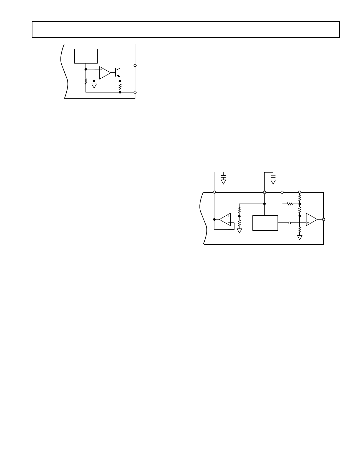
Current Amplifier
The DAC output current drives the second section, an opera-
tion amplifier and NPN transistor which acts as a current
amplifier to set the current flowing through the LOOP RTN
pin. Figure 4 shows the current amplifier section of the AD421.
An 80 k
Ω
resistor connected between the DAC output and loop
return is used as a sampling resistor to determine current. The
base drive to the NPN transistor servos the voltage across the
40
Ω
resistor to equal the voltage across the 80 k
Ω
resistor.
CIRCUIT DESCRIPTION
The AD421 is designed for use in loop-powered 4–20 mA smart
transmitter applications. A smart transmitter, as a remote
instrument, controls its current output signal on the same pair
of wires from which it receives its power. The AD421 essentially
provides three primary functions in the smart transmitter. These
functions are a DAC function for converting the microprocessor/
microcontroller’s digital data to analog format, a current amp-
lifier which sets the current flowing in the loop and a voltage
regulator to provide a stable operating voltage from the loop
supply. The part also contains a high speed serial interface, two
buffered output references and a clock oscillator circuit. The
different sections of the AD421 are discussed in more detail
below.
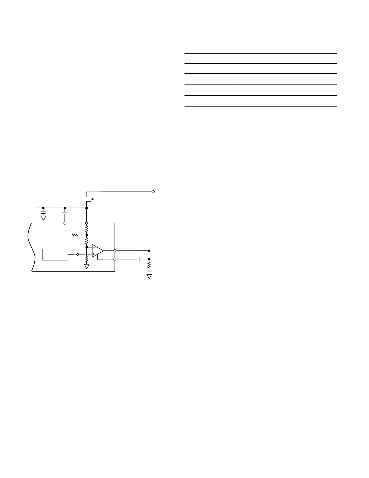
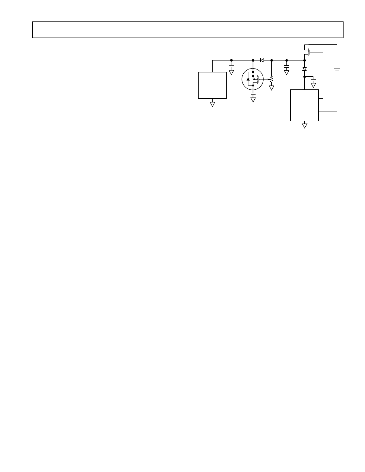
Voltage Regulator
The voltage regulator consists of an op amp, bandgap reference
and an external depletion mode FET pass transistor. This cir-
cuit is required to regulate the loop voltage that powers the
AD421 itself and the rest of the transmitter circuitry. Figure 3
shows the voltage regulator section of the AD421 plus the associ-
ated external circuitry for a V
CC
of 3.3 V.
1.21V
112.5k
Ω
134k
Ω
75k
Ω
121k
Ω
V
CC
LV
10µF
COM
V
CC
TO EXTERNAL
CIRCUITRY
DN25D
DRIVE
COMP
0.01µF
1k
Ω
1000pF
LOOP(+)
BANDGAP
REFERENCE
AD421
0.01µF
Figure 3. AD421 Voltage Regulator Circuit to Provide
V
CC
= 3.3 V
The signal on the LV pin selects the voltage to which V
CC
regulates by changing the gain of the resistor divider between
the op amp inverting input and the V
CC
pin. As the LV pin
varies between COM and V
CC
, the voltage from the regulator
loop varies between 3 V and 5 V nominal. With LV connected
to COM, the regulated voltage is 5 V; with LV connected
through a 0.01
µ
F capacitor to V
CC
, the regulated voltage is
3.3 V while if LV is connected to V
CC
, the regulated voltage is
3 V.
The range of loop voltages that can be used by the configuration
shown in Figure 3 is determined by the FET breakdown and
saturation voltages. The external FET parameters such as Vgs
(off), I
DSS
and transconductance must be chosen so that the op
amp output on the DRIVE pin can control the FET operating
point while swinging in the range from V
CC
to COM.
The main characteristics for selecting the FET pass transistor
are as follows:
AD421
–7–
REV. 0
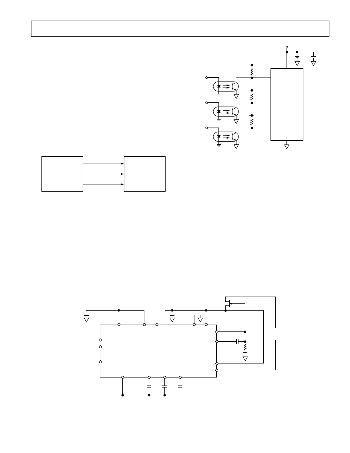
Reference Section
The AD421 contains an on-chip 1.21 V bandgap reference
which is used as part of the voltage regulator loop. A bandgap
reference is also used to generate two references voltages
which are available for use external to the AD421. Figure 5
shows the reference section of the AD421. The REF OUT1 pin
provides a buffered +1.25 V reference voltage which can supply
up to 0.5 mA of external current. The REF OUT2 pin provides
a +2.5 V reference voltage which is also capable of providing
0.5 mA of external current. To use the AD421 with its own
reference, simply connect the REF OUT2 pin to the REF IN
pin of the device. Alternatively, the part can be used with an
external reference by connecting the external reference between
REF IN and COM.
When REF OUT1 and REF OUT2 are used in application
circuits, external 4.7
µ
F capacitors are required on the reference
pins to provide compensation and ensure stable operation of the
references. These capacitors can be omitted if the internal
references are not required.
1.21V
112.5k
Ω
134k
Ω
75k
Ω
121k
Ω
V
CC
LV
4.7µF
DRIVE
2.5V
BANDGAP
REFERENCE
AD421
50k
Ω
REF OUT2
(2.5V)
50k
Ω
4.7µF
REF OUT1
(1.25V)
Figure 5. Reference Section
REF OUT2 is sensed internally, and if more than 0.5 mA is
drawn externally from this reference, the chip goes into a power
on reset state. In this state the sigma-delta DAC is disabled, the
internal oscillator is stopped and the input data latch is cleared.
REF OUT1 has limited current sinking capability. If REF
OUT1 is required to sink current, a resistive load of 100 k
Ω
to COM should be added in addition to the 4.7
µ
F capacitor.
USING THE AD421
The AD421 can be programmed for normal 4–20 mA operation
or for alarm current operation. For normal operation, the
coding is 16-bit straight (natural) binary over an output current
range of 4 mA to 20 mA. For alarm current operation, the
coding is also straight binary but with 17 bits of resolution over
twice the span, 0 mA to 32 mA, although the part should not be
programmed outside the range of 3.5 mA to 24 mA. To deter-
mine whether data written to the part is normal 4–20 mA data
or alarm current data, the number of clock pulses between two
successive LATCH pulses are counted.
4–20 mA Coding
Table II shows the ideal input-code-to-output-current relation-
ship for normal operation of the AD421. The output current
values shown assume a REF IN voltage of +2.5 V. With a
REF IN of +2.5 V, 1 LSB = 16 mA/65,536 = 244 nA. Figure 6
shows a timing diagram for programming the AD421 for normal
4–20 mA operation, the AD421 outputting a current of
11.147 mA. With 16 clock pulses between consecutive latch
signals data written is for normal 4–20 mA operation.
AD421
BOOST
40
Ω
80k
Ω
LOOP RTN
SWITCHED
CURRENT
SOURCES
Figure 4. Current Amplifier
The BOOST pin is normally tied to the V
CC
pin. As the DAC
input code varies from all zeroes to full scale, the output current
from the NPN transistor and thus the total loop current varies
from 4 mA to 20 mA. With BOOST and V
CC
tied together, the
external FET (DN25D) has to supply the full range of loop
current (4 mA to 20 mA).
Digital Interface
The digital interface on the AD421 consists of just three wires:
DATA, CLOCK and LATCH. The interface connects directly
to the serial ports of commonly-used microcontrollers without
the need for any external glue logic. Data is loaded MSB first
into an input shift register on the rising edge of the CLOCK
signal and is transferred to the DAC latch on the rising edge of
the LATCH signal. The timing diagrams for the serial interface
are shown in Figure 1 and Figure 2.
The data to be loaded to the AD421’s input shift register takes
two forms; normal 4–20 mA data or alarm current data. The
first form is where the AD421 operates over its normal 4 mA to
20 mA output range with 16 bits of resolution between these
endpoints. The second form allows the user to program a
current value outside this range as an indication from the
transmitter than there is a problem with the transducer. The
AD421 counts the number of clock pulses which it receives
between LATCH signals as a means of determining whether the
data clocked in is 4–20 mA data or alarm current data.
If there are 16 rising clock edges between successive LATCH
pulses, then the data being loaded to the input shift register is
assumed to be normal 4–20 mA data. On the rising edge of the
LATCH signal, the input shift register data is transferred to the
DAC latch in a 16-bit parallel transfer. In this case, the 16 bits
of data in the DAC latch program the output current between
4 mA for all 0s and 20 mA for all 1s (see Table II). Data
transferred to the AD421 should be MSB first.
If there are more than 16 clock pulses between successive
LATCH pulses, then the data being loaded to the input shift
register is assumed to be alarm current data. In this case, the
AD421 accepts 17 bits of data into its shift register. For situa-
tions where there are more than 17 clocks in the serial write
operation (for example, 24 clocks in a 3
×
8-bit transfer from the
serial port of a microcontroller) the AD421 simply accepts the
last 17 bits of the serial write operation. Data transferred in this
serial write operation is LSB last (i.e., the MSB is loaded on the
17th rising clock edge prior to the LATCH pulse). On the rising
edge of the LATCH signal, the input shift register data is
transferred to the DAC latch in a 17-bit parallel transfer. In this
case, the 17 bits of data in the DAC latch program the output
current between 0 mA for all 0s and 32 mA for all 1s (see Table
III). However, in practice the AD421 cannot reliably produce a
current less than 3.5 mA or more than 24 mA.
AD421
–8–
REV. 0
WORD "N"
0
1
1
0 0
1 1
0
0
0
0
0
0
0
0
0
0
CLOCK
DATA
(MSB)
(LSB)
B15
B14
B13
B12
B1
1
B10
B9
B8
B7
B6
B5
B4
B3
B2
B1
B0
LATCH
B16
X X X X X X X
X
X
X
X
X
X
X
Figure 7. Write Cycle for Programming Alarm Current
Data
MICROPROCESSOR INTERFACING
AD421 – MC68HC11 (SPI BUS) INTERFACE
Figure 8 shows a typical interface between the AD421 and the
Motorola MC68HC11 SPI (Serial Peripheral Interface) bus.
The SCK, MOSI and SS pins of the 68HC11 are respectively
connected to the CLOCK, DATA IN and LATCH pins of the
AD421.
SCK
MOSI
SS
CLOCK
DATA IN
LATCH
AD421*
68HC11
* ADDITIONAL PINS OMITTED FOR CLARITY
Figure 8. AD421 to 68HC11 Interface
A typical routine such as the one shown below begins by initializ-
ing the state of the various SPI data and control registers.
INIT
LDAA #$2F
;SS = 1; SCK = 0; MOSI = 1
STAA
PORTD
;SEND TO SPI OUTPUTS
LDAA #$38
;SS, SCK,MOSI = OUTPUTS
STAA
DDRD
;SEND DATA DIRECTION INFO
LDAA #$50
;DABL INTRPTS,SPI IS MASTER & ON
STAA
SPCR
;CPOL = 0, CPHA = 0, 1MHZ BAUDRATE
NEXTPT LDAA MSBY
;LOAD ACCUM W/UPPER 8 BITS
BSR
SENDAT ;JUMP TO DAC OUTPUT ROUTINE
JMP
NEXTPT ;INFINITE LOOP
SENDAT LDY
#$1000
;POINT AT ON-CHIP REGISTERS
BCLR
$08,Y,$20 ;DRIVE SS (LATCH) LOW
STAA
SPDR
;SEND MS-BYTE TO SPI DATA REG
WAIT1
LDAA SPSR
;CHECK STATUS OF SPIE
BPL
WAIT1
;POLL FOR END OF X-MISSION
LDAA LSBY
;GET LOW 8 BITS FROM MEMORY
STAA
SPDR
;SEND LS-BYTE TO SPI DATA REG
WAIT2
LDAA SPSR
;CHECK STATUS OF SPIE
BPL
WAIT2;
;POLL FOR END OF X-MISSION
BSET
$08,Y,$20 ;DRIVE SS HIGH TO LATCH DATA
RTS
The SPI data port is configured to process data in 8-bit bytes.
The most significant data byte (MSBY) is retrieved from
memory and processed by the SENDAT routine. The SS pin is
driven low by indexing into the PORTD data register and clear
Bit 5. The MSBY is then sent to the SPI data register where it is
Table II. Ideal Input/Output Code Table
for 4–20 mA Operation
Code
Output Current
0000 0000 0000 0000
4 mA
0000 0000 0000 0001
4.000244 mA
0000 0000 0000 0010
4.000488 mA
0100 0000 0000 0000
8 mA
1000 0000 0000 0000
12 mA
1100 0000 0000 0000
16 mA
1111 1111 1111 1101
19.999268 mA
1111 1111 1111 1110
19.999512 mA
1111 1111 1111 1111
19.999756 mA
WORD "N"
WORD "N +1"
1
0
1 1
1
1
1
1 1
1
0
0
0
0
0 0
1
0 0
1
CLOCK
DATA
(MSB)
(LSB)
B15
B14
B13
B12
B1
1
B10
B9
B8
B7
B6
B5
B4
B3
B2
B1
B0
B15
B14
B13
B12
LATCH
Figure 6. Write Cycle for 4–20 mA Operation
Alarm Current Coding
Table III shows the ideal input-code-to-output-current relation-
ship for alarm current programming of the AD421. In this case,
the equivalent span is 0 mA to 32 mA but a reliable operating
span is 3.5 mA to 24 mA. The part may give an indeterminate
output for code values outside the range given in the table. As a
result, the user is advised to restrict the code programmed to the
part in alarm current mode to within the range shown in Table
III. Figure 7 shows a timing diagram for loading an alarm
current of 3.75 mA to the AD421 with an 8-bit microcontroller
using three 8-bit writes.
The output current values shown assume a REF IN voltage of
+2.5 V. With a REF IN of +2.5 V, an ideal 1 LSB = 32 mA/
131,072 = 244 nA.
Table III. Ideal Input/Output Code Table
for Alarm Current Operation
Code
Output Current
0 0011 1000 0000 0000
3.5 mA
0 0011 1100 0000 0000
3.75 mA
0 0100 0000 0000 0000
4 mA
0 1000 0000 0000 0000
8 mA
1 0000 0000 0000 0000
16 mA
1 0100 0000 0000 0000
20 mA
1 0110 0000 0000 0000
22 mA
1 1000 0000 0000 0000
24 mA
AD421
–9–
REV. 0
automatically transferred to the AD421 internal shift resister.
The HC11 generates the requisite eight clock pulses with data
valid on the rising edges. After the MSBY is transmitted, the
least significant byte (LSBY) is loaded from memory and
transmitted in a similar fashion. To complete the transfer, the
LATCH pin is driven high when loading the complete 16-bit
word into the AD421.
AD421 TO MICROWIRE INTERFACE
The flexible serial interface of the AD421 is also compatible
with the National Semiconductor MICROWIRE interface. The
MICROWIRE interface is used in microcontrollers such as the
COP400 and COP800 series of processors. A generic interface
to use the MICROWIRE interface is shown in Figure 9. The
G1, SK, and SO pins of the MICROWIRE interface respec-
tively connected to the LATCH, CLOCK, and DATA IN pins
of the AD421.
SK
SO
CLOCK
DATA IN
LATCH
AD421*
MICROWIRE
* ADDITIONAL PINS OMITTED FOR CLARITY
G1
Figure 9. AD421 to MICROWIRE Interface
Opto-Isolated Interface
The AD421 has a versatile serial 3-wire serial interface making
it ideal for minimizing the number of control lines required for
isolation of the digital system from the control loop. In intrinsi-
cally safe applications or due to noise, safety requirements, or
distance, it may be necessary to isolate the AD421 from the
controller. This can easily be achieved by using opto-isolators.
Figure 10 shows an opto-isolated interface to the AD421 where
CLOCK, DATAIN and LATCH are driven from opto-couplers.
Be aware of signal inversion across the opto-couplers.
0.1µF
10µF
V
CC
10k
Ω
V
CC
10k
Ω
V
CC
10k
Ω
V
CC
CLOCK
LATCH
DATA IN
AD421*
COM
CLOCK
LATCH
DATA IN
V
CC
Figure 10. Opto-Isolated Interface
APPLICATIONS SECTION
Basic Operating Configuration
Figure 11 shows the basic connection diagram for the AD421
operating at 5 V. This circuit shows the minimum of external
components to operate the AD421. In the diagram, the AD421’s
regulator loop in conjunction with the DN25D pass transistor
provides the V
CC
voltage for the AD421 itself and for other
devices in the trans-mitter. The V
CC
pin should be well decou-
pled with a 10
µ
F capacitor to ensure regulator stability and to
absorb power glitches on the V
CC
line of the AD421 and other
devices in the system. If the AD421 is operated with V
CC
= 3 V,
the transfer function shifts negative. To correct for this a 16 k
Ω
resistor connected between COM and LOOPRTN will approxi-
mately compensate for the V
CC
supply sensitivity in moving from
5 V to 3 V by adjusting the gain of the AD421.
Figure 11. Basic Connection Diagram
C1
C2
C3
COM
COM TO EXTERNAL
CIRCUITRY
V
CC
LV
10µF
COM
V
CC
TO EXTERNAL
CIRCUITRY
DN25D
DRIVE
COMP
0.01µF
1k
Ω
1000pF
BOOST
LOOP RTN
V
LOOP
0.01µF
0.01µF
0.0033µF
LATCH
CLOCK
DATA
REF IN
REF OUT2
REF OUT1
4.7µF
COM
AD421
AD421
–10–
REV. 0
A capacitor of 0.01
µ
F connected between COMP and DRIVE
is required to stabilize the feedback loop formed with the
regulator op amp and the external pass transistor. An external
snubber circuit of 1 k
Ω
and 1000 pF is required between the
DRIVE pin and COM and a 0.1
µ
F cap between COMP and
DRIVE to stabilize the feedback loop formed by the regulator
op amp and the external pass transistor.
The internal 2.5 V reference on the AD421 is used as the
reference for the AD421 and this has to be decoupled with a
4.7
µ
F capacitor for compensation and stability purposes. The
sigma-delta DAC on the part consists of a second order modu-
lator followed by a continuous time filter. The resistors for each
of the filter sections are on-chip while the capacitors are external
on the C1 to C3 pins. To meet the specified full-scale settling
on the part, low dielectric absorption capacitors (NPO) are
required. Suitable values for these capacitors are C1 = C2 =
0.01
µ
F, and C3 = 0.0033
µ
F.
The digital interface on the AD421 consists of just three wires:
DATA, CLOCK and LATCH. The interface connects directly
to the serial ports of commonly-used microcontrollers without
the need for any external glue logic. Data is loaded into an input
shift register on the rising edge of the CLOCK signal and is
transferred to the DAC latch on the rising edge of the LATCH
signal.
Reduce Power Load on External FET
Figure 12 shows a circuit where an external NPN transistor is
added to reduce the power loading on the FET. The FET will
supply the V
CC
and an external high voltage NPN bipolar
transistor can carry the BOOST current. The BOOST pin sinks
the necessary current from the loop so that the current flowing
into BOOST plus the current flowing into COM is equal to the
programmed loop current. The external NPN transistor reduces
the external power load that the FET has to carry to less than
750
µ
A if no other components share the V
CC
line and to less
than 4 mA in applications that share the same V
CC
line as the
AD421.
1.21V
112.5k
Ω
134k
Ω
75k
Ω
121k
Ω
V
CC
LV
10µF
COM
V
CC
TO EXTERNAL
CIRCUITRY
DN25D
DRIVE
COMP
0.01µF
1k
Ω
1000pF
LOOP(+)
BANDGAP
REFERENCE
AD421
BC639/BC337
BOOST
40
Ω
80k
Ω
LOOP RTN
LOOP(–)
Figure 12. External NPN Transistor Reduces Power Load
on FET
Smart Transmitter
The AD421 is intended for use in 4 to 20 mA smart transmit-
ters. A smart transmitter is a system that incorporates a
microprocessor system which is used for linearization and
communication. Figure 13 shows a block diagram of a typical
smart transmitter. In this example, the transmitter does not have
any digital communication capabilities.
4 TO 20mA
MEASUREMENT
CIRCUIT
MICRO-
PROCESSOR
D/A
CONVERTER
A/D
CONVERTER
MEMORY
SENSORS
Figure 13. Typical Smart Transmitter
Figure 14 shows a typical smart transmitter application circuit
using the AD421.
The sensor voltage to be measured at the transmitter is con-
verted using a high resolution sigma-delta converter such as
the AD7714 or AD7715. These devices have an on-board PGA
which can provide gains on the analog front end from 1 to 128.
This allows for an analog input range as low as 10 mV which
allows the transducer to be connected directly to the ADC. The
AD7714/AD7715 have digital calibration techniques which are
used to eliminate gain and offset errors. In addition, back-
ground calibration techniques are provided whereby the part
continually calibrates itself and the user does not have to
worry about issuing periodic calibration commands to remove
effects of time and temperature drift.
In normal operation the microprocessor reads the data from the
AD7714/AD7715. After the data is processed by the micro-
controller, the data is transferred from the serial port of the
processor to the AD421 for transmission over the 4 to 20 mA
loop back to the control center.
The AD421 regulates the loop voltage to create power for the
rest of the transmitter circuitry. In Figure 14, the derived V
CC
voltage is 3.3 V which is achieved by connecting the LV pin to
V
CC
through 0.01
µ
F. REF OUT2 provides the reference voltage
for the AD421 itself while REF OUT1 provides the reference
voltage for the AD7714 /AD7715.
AD421
–11–
REV. 0
DV
DD
AV
DD
REF IN
CS
DATA OUT
SCLK
DATA IN
AGND
DGND
MCLK IN
MCLK OUT
AD7714/
AD7715
ANALOG
TO
DIGITAL
CONVERTER
SENSORS
RTD
mV
Ω
TC
4.7µF
REF OUT1
BOOST
V
CC
LV
COMP
DRIVE
LOOP
RTN
REF OUT2
REF IN
CLOCK
LATCH
DATA
COM
C1
C2
C3
LOOP
POWER
0.01µF
DN25D
10µF
3.3V
1.25V
4.7µF
AMBIENT
TEMP
SENSOR
AD421
MICROCONTROLLER
V
CC
GND
0.01µF
1k
Ω
1000pF
0.1µF
100k
Ω
Figure 14. AD421 in Smart Transmitter Application
Figure 16 shows a block diagram of a smart and intelligent
transmitter. An intelligent transmitter is a transmitter in which
the functions of the microprocessor are shared between deriving
the primary measurement signal, storing information regarding
the transmitter itself, its application data and its location and
also managing a communication system which enables two way
communication to be superimposed on the same circuit that
carries the measurement signal. A smart transmitter incorporat-
ing the HART protocol is an example of a smart intelligent
transmitter.
4 TO 20mA
MEASUREMENT
CIRCUIT
MICRO-
PROCESSOR
D/A
CONVERTER
A/D
CONVERTER
MEMORY
SENSORS
COMMUNICATION
SYSTEM
Figure 16. Smart and Intelligent Transmitter
Figure 17 shows an example of the AD421 in a HART transmit-
ter application. Most of the circuit is as outlined in the smart
transmitter as shown in Figure 14. The HART data transmitted
on the loop is received by the transmitter using a bandpass filter
and modem and the HART data is transferred to the micro-
controller’s UART or asynchronous serial port. HART data to
be transmitted on the loop is sent from the microcontroller’s
UART or asynchronous serial port to the modem. It is then
waveshaped before being coupled onto the AD421’s output at
the C3 pin. The value of the coupling capacitor C
C
is deter-
mined by the waveshaper output and the C3 capacitor of the
AD421. The blocks containing the Bell 202 Modem, waveshaper
and bandpass filter come in a complete solution with the 20C15
from Symbios Logic, Inc., or HT2012 from SMAR Research
Corp.
HART Interfacing
The HART protocol uses a frequency shift (FSK) keying
technique based on the Bell 202 Communication Standard which
is one of several standards used to transmit digital signals over
the telephone lines. This technique is used to superimpose
digital communication on to the 4 to 20 mA current loop
connecting the central system to the transmitter in the field.
Two different frequencies, 1200 Hz and 2200 Hz, are used to
represent binary 1 and 0 respectively, as shown in Figure 15.
These sine wave tones are superimposed on the dc signal at a
low level with the average value of the sine wave signal being
zero. This allows simultaneous analog and digital communica-
tions. Additionally, no dc component is added to the existing
4 to 20 mA signal regardless of the digital data being sent over
the line. Consequently, existing analog instruments continue to
work in systems that implement HART as the low-pass filtering
usually present effectively removes the digital signal. A single
pole 10 Hz low-pass filter effectively reduces the communication
signal to a ripple of about
±
0.01% of the full-scale signal. The
HART protocol specifies that master devices like a host control
system or a hand held terminal transmit a voltage signal whereas
a slave or field device transmits a current signal. The current
signal is converted into a corresponding voltage by the loop load
resistor.
APPROX
+0.5mA
APPROX
–0.5mA
1200Hz
“1”
2200Hz
“0”
Figure 15. HART Transmission of Digital Signals
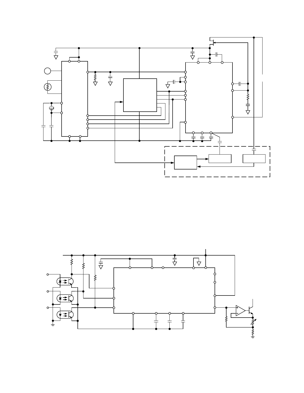
AD421
–12–
REV. 0
DV
DD
AV
DD
REF IN
CS
DATA OUT
SCLK
DATA IN
AGND
DGND
MCLK IN
MCLK OUT
AD7714/
AD7715
ANALOG
TO
DIGITAL
CONVERTER
SENSORS
RTD
mV
Ω
TC
REF OUT1
BOOST
V
CC
LV
COMP
DRIVE
LOOP
RTN
REF OUT2
REF IN
CLOCK
LATCH
DATA
COM
C1
C2
C3
LOOP
POWER
0.01µF
DN25D
10µF
3.3V
1.25V
4.7µF
AMBIENT
TEMP
SENSOR
AD421
MICROCONTROLLER
V
CC
GND
WAVEFORM
SHAPER
BANDPASS
FILTER
HART
MODEM
BELL 202
0.1µF
0.01µF
1k
Ω
1000pF
C
C
HT20C12/20C15
4.7µF
100k
Ω
Figure 17. AD421 in HART Transmitter Application
R2. The ratio of R1 to R2 determines the current that flows in
the load resistor R
L
. I
L
= [1 + R1/R2]
×
I
PROG
, where I
L
is the
current that flows in the load resistor R
L
and I
PROG
is the current
programmed to the AD421. R1 and R2 are external to the
AD421 and will need to be matched resistors to obtain a highly
accurate current source.
LOOP
RTN
R2
R
L
R1
C1
C2
C3
COM
COM TO EXTERNAL
CIRCUITRY
V
CC
LV
10µF
COM
DRIVE
COMP
BOOST
0.01µF
0.01µF
0.0033µF
LATCH
CLOCK
DATA
REF IN
REF OUT2
REF OUT1
4.7µF
COM
AD421
V
S
+5V
10k
Ω
10k
Ω
10k
Ω
CLOCK
LATCH
DATA
V
S
RETURN
Figure 18. AD421 in Programmable Current Source/Sink
Current Source
Figure 18 shows an application circuit for the AD421 being
used as a current source. The current programmed to the
AD421 (4 to 20 mA) will develop a voltage across R1. This
same voltage due to negative feedback will be generated across
AD421
–13–
REV. 0
Battery Backup
Figure 19 shows an application circuit for the AD421 where the
micro and memory sections of the circuitry are protected against
losing data if the loop is broken. The backup circuit switches
from V
CC
to battery voltage without a glitch when V
CC
power is
lost. The IRFF9113 acts as a current source during normal
operation and provides a constant charging current to the
supercap or Nicad. The loss of V
CC
drops the IRFF9113’s gate
voltage to zero volts, which allows the battery or supercaps
current to flow through the MOSFETs channel and integral
body diode to provide power for the micro and memory sections.
To calibrate this circuit, connect an ammeter in series with the
battery or supercap. Then with V
CC
and the load present adjust
the 100 k
Ω
potentiometer for the battery charging current
recommended by the battery or supercap manufacturer.
Nonrechargeable batteries should not be used in this application
due to danger of explosion.
100k
Ω
IN3611
IN3611
DN25D
V
CC
DRIVE
LOOP
RTN
COM
AD421*
V
LOOP
IRFF9113
SUPERCAP
V
CC
GND
MICRO/
MEMORY
*ADDITIONAL CIRCUITRY OMITTED FOR CLARITY
4.7µF
4.7µF
0.1µF
Figure 19. Battery Backup Circuit

AD421
–14–
REV. 0
INDEX
FEATURES . . . . . . . . . . . . . . . . . . . . . . . . . . . . . . . . . . . . 1
GENERAL DESCRIPTION . . . . . . . . . . . . . . . . . . . . . . . . 1
PRODUCT HIGHLIGHTS . . . . . . . . . . . . . . . . . . . . . . . . 1
AD421–LOOP-POWERED SPECIFICATIONS . . . . . . . . 2
AD421–DAC SPECIFICATIONS . . . . . . . . . . . . . . . . . . . 2
TIMING CHARACTERISTICS . . . . . . . . . . . . . . . . . . . . 3
ABSOLUTE MAXIMUM RATINGS . . . . . . . . . . . . . . . . 4
PIN CONFIGURATION . . . . . . . . . . . . . . . . . . . . . . . . . . 4
PIN FUNCTION DESCRIPTION . . . . . . . . . . . . . . . . . . 5
CIRCUIT DESCRIPTION . . . . . . . . . . . . . . . . . . . . . . . . 6
Voltage Regulator . . . . . . . . . . . . . . . . . . . . . . . . . . . . . . . 6
FET Characteristics . . . . . . . . . . . . . . . . . . . . . . . . . . . . . 6
DAC Section . . . . . . . . . . . . . . . . . . . . . . . . . . . . . . . . . . 6
Current Amplifier . . . . . . . . . . . . . . . . . . . . . . . . . . . . . . . 6
Digital Interface . . . . . . . . . . . . . . . . . . . . . . . . . . . . . . . . 7
Reference Section . . . . . . . . . . . . . . . . . . . . . . . . . . . . . . . 7
USING THE AD421 . . . . . . . . . . . . . . . . . . . . . . . . . . . . . 7
4–20 mA CODING . . . . . . . . . . . . . . . . . . . . . . . . . . . . . 7
Alarm Current Coding . . . . . . . . . . . . . . . . . . . . . . . . . . . 8
MICROPROCESSOR INTERFACING . . . . . . . . . . . . . . . 8
APPLICATIONS SECTION . . . . . . . . . . . . . . . . . . . . . . . 9
Basic Operating Configuration . . . . . . . . . . . . . . . . . . . . . 9
Reduce Power Loading on External FET . . . . . . . . . . . . 10
Smart Transmitter . . . . . . . . . . . . . . . . . . . . . . . . . . . . . 10
HART Interfacing . . . . . . . . . . . . . . . . . . . . . . . . . . . . . 11
Current Source . . . . . . . . . . . . . . . . . . . . . . . . . . . . . . . 12
Battery Backup . . . . . . . . . . . . . . . . . . . . . . . . . . . . . . . . 13
MECHANICAL INFORMATION . . . . . . . . . . . . . . . . . . 15
AD421
–15–
REV. 0
OUTLINE DIMENSIONS
Dimensions shown in inches and (mm).
16-Lead Plastic DIP
(N-16)
16
1
8
9
0.840 (21.33)
0.745 (18.93)
0.280 (7.11)
0.240 (6.10)
PIN 1
SEATING
PLANE
0.022 (0.558)
0.014 (0.356)
0.060 (1.52)
0.015 (0.38)
0.210 (5.33)
MAX
0.130
(3.30)
MIN
0.070 (1.77)
0.045 (1.15)
0.100
(2.54)
BSC
0.160 (4.06)
0.115 (2.93)
0.325 (8.25)
0.300 (7.62)
0.015 (0.381)
0.008 (0.204)
0.195 (4.95)
0.115 (2.93)
16-Lead (Wide Body) Small Outline Package
(R-16)
16
9
8
1
0.4133 (10.50)
0.3977 (10.00)
0.4193 (10.65)
0.3937 (10.00)
0.2992 (7.60)
0.2914 (7.40)
PIN 1
SEATING
PLANE
0.0118 (0.30)
0.0040 (0.10)
0.0192 (0.49)
0.0138 (0.35)
0.1043 (2.65)
0.0926 (2.35)
0.0500
(1.27)
BSC
0.0125 (0.32)
0.0091 (0.23)
0.0500 (1.27)
0.0157 (0.40)
8
°
0
°
0.0291 (0.74)
0.0098 (0.25)
x 45
°
16-Lead Thin Shrink Small Outline Package (TSSOP)
(RU-16)
16
9
8
1
0.201 (5.10)
0.193 (4.90)
0.256 (6.50)
0.246 (6.25)
0.177 (4.50)
0.169 (4.30)
PIN 1
SEATING
PLANE
0.006 (0.15)
0.002 (0.05)
0.0118 (0.30)
0.0075 (0.19)
0.0256
(0.65)
BSC
0.0433
(1.10)
MAX
0.0079 (0.20)
0.0035 (0.090)
0.028 (0.70)
0.020 (0.50)
8
°
0
°

PRINTED IN U.S.A.
C2105–18–1/96
–16–