

a
Electrically Induced Damage to Standard Linear Integrated Circuits:
The Most Common Causes and the Associated Fixes to Prevent Reoccurrence
by Niall Lyne
AN-397
APPLICATION NOTE
ONE TECHNOLOGY WAY
•
P.O. BOX 9106
•
NORWOOD, MASSACHUSETTS 02062-9106
•
617/329-4700
INTRODUCTION
The sensitivity of electronic components to transient
electrical overstress events is a well-known problem,
exacerbated by the continuing evolution of integrated
circuits. Smaller geometries, increased circuit densities,
and the limited area allotted to on-chip protection all
tend to increase this sensitivity. In an effort to minimize
costs in each particular segment of system implementa-
tion, the burden of transient protection is often shifted to
other, less efficient means.
Techniques for protection from “zapping” depend on
the stage of manufacture. During the manufacturing of
integrated circuits and assembly of electronic equip-
ment, protection is achieved through the use of well-
known measures such as static dissipative table tops,
wrist straps, ionized air blowers, antistatic shipping
tubes, etc. These methods will be discussed only briefly
here in relation to Electrostatic Discharge (ESD) protec-
tion. Likewise this application note is not addressed to
precautionary measures employed during shipping, in-
stallation, or repair of equipment. Rather, the main
thrust will be limited to protection aspects called upon
during printed circuit board assembly, normal operation
of the equipment (often by operating personnel who are
untrained in preventative measures), and in service con-
ditions where the transient environment may not be well
characterized.
The transient environment varies widely. There are sub-
stantial differences among those experienced by, say,
automotive systems, airborne or shipborne equipment,
space systems, industrial equipment or consumer prod-
ucts. All types of electronic components can be
destroyed or degraded.
1
Even capacitors, relays, con-
nectors, printed circuit boards, etc., are susceptible,
although their threshold levels are much higher than
integrated circuits. Microwave diodes and transistors
are among the most sensitive components. However,
this application note will be restricted to standard linear
integrated circuits because of their wide usage, and to
limit the scope of coverage.
This application note will first review the nature of the
threat to integrated circuits in an operating environ-
ment, and then briefly discuss overall device protection
from the following: (1)
ESD events caused by human
handling, automatic board insertion equipment, etc., (2)
LATCH-UP generated from power-up/down sequencing
errors, floating ground(s) due to a loose edge connec-
tors, etc., and finally, (3)
HIGH VOLTAGE TRANSIENTS
generated from a power supply, a defective circuit
board, during circuit board troubleshooting, etc.
Electrostatic Discharge
Electrostatic discharge is a single, fast, high current
transfer of electrostatic charge that results from:
•
Direct contact transfer between two objects at differ-
ent potentials,
or
•
A high electrostatic field between two objects when
they are in close proximity.
The prime sources of static electricity are mostly insula-
tors and are typically synthetic materials, e.g., vinyl or
plastic work surfaces, insulated shoes, finished wood
chairs, Scotch tape, bubble pack, soldering irons with
ungrounded tips, etc. Voltage levels generated by these
sources can be extremely high since their charge is not
readily distributed over their surfaces or conducted to
other objects.
The generation of static electricity caused by rubbing
two substances together is called the triboelectric effect.
Examples of sources of triboelectric electrostatic charge
generation in a high RH (
≈
60%) environment include:
•
Walking across a carpet
⇒
1000 V–1500 V generated.
•
Walking across a vinyl floor
⇒
150 V–250 V generated.
•
Handling material protected by clear plastic covers
⇒
400 V–600 V generated.
•
Handling polyethylene bags
⇒
1000 V–1200 V generated.
•
Pouring polyurethane foam into a box
⇒
1200 V–
1500 V generated.
–2–
•
ICs sliding down an open antistatic shipping tube
⇒
25 V–250 V generated.
Note: For low RH (<30%) environments, generated volt-
ages can be >10
×
those listed above.
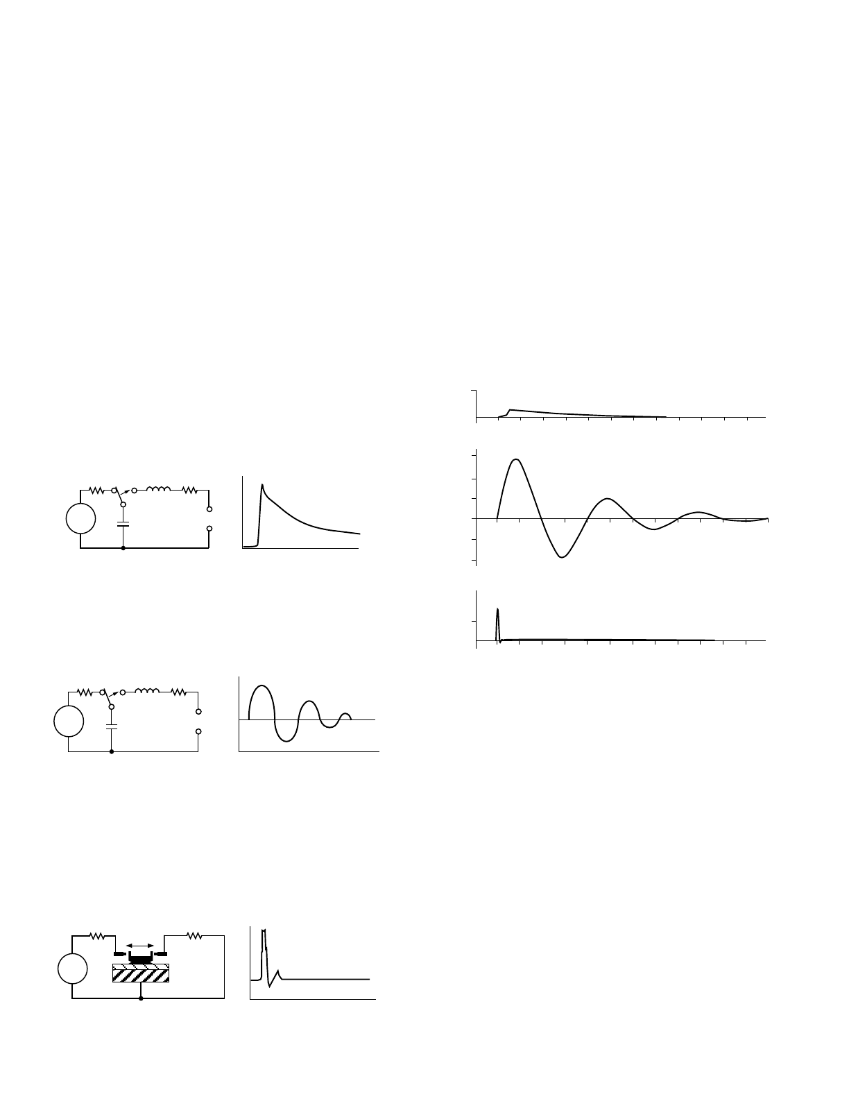
ESD Models
To evaluate the susceptibility of devices to simulated
stress environments a host of test waveforms have been
developed. The three most prominent of these wave-
forms currently in general use for simulating ESD events
in semiconductor or discrete devices are: The Human
Body Model (HBM), the Machine Model (MM), and the
Charged Device Model (CDM). The test circuits and cur-
rent waveform characteristics for these three models
are shown in Figures 1 to 3. Each of these models repre-
sents a fundamentally different ESD event. Conse-
quently, correlation between the test results for these
models is minimal.
Human Body Model:
2
Simulates the discharge event that occurs when a per-
son charged to either a positive or negative potential
touches an IC at a different potential.
RLC = 1.5 k
Ω
, ~0 nH, 100 pF.
HVPS
10M
Ω
0H
1.5k
Ω
100pF
S1
DUT
I
t
Figure 1. Human Body Model
Machine Model:
Japanese model based on a worst-case HBM.
RLC = 0
Ω
, 500 nH, 200 pF.
I
t
HVPS
10M
Ω
500nH
0k
Ω
200pF
S1
DUT
Figure 2. Machine Model
Charged Device Model:
Simulates the discharge that occurs when a pin on an IC
charged to either a positive or negative potential con-
tacts a conductive surface at a different (usually ground)
potential.
RLC = 0
Ω
, ~0 nH, 1 pF–20 pF.
HVPS
1G
Ω
1
Ω
DIELECTRIC
GROUND PLANE
DISCHARGE
CHARGE
I
t
Figure 3. Charged Device Model
Comparison of HBM, MM, and CDM Waveforms
Figure 4 shows 400 V HBM, MM, and CDM discharge
waveforms on the same current vs. time scale. These
waveforms are of great use in predicting what failure
mechanism may result on a particular device type due to
ESD events simulated by one of these three models.
The rise time for the HBM waveform is <10 ns (typically
6 ns–9 ns), and this waveform decays exponentially to-
wards 0 V with a fall time of >150 ns. MIL-STD-883
3
Method 3015
Electrostatic Discharge Sensitivity Classifi-
cation requires a rise time of <10 ns and a delay time of
150
±
20 ns (Method 3015 defines delay time as the time
for the waveform to drop from 90% of the peak current
to 36.8% of the peak current). The peak current for the
HBM waveform is
≈
400 V/1500
Ω
or 0.267A. Although
this peak current is much lower than that for 400
V CDM
and MM events, the relatively long duration of the total
HBM event results in a discharge of relatively high
energy.
AMPS
2
HBM
20ns/DIV
t
6
4
2
0
–2
–4
AMPS
MM
20ns/DIV
t
2
AMPS
CDM
20ns/DIV
t
Figure 4. Relative Comparison of 400 V HBM, MM,
and CDM Discharges
The MM waveform consists of both positive-going and
negative-going sinusoidal peaks with peak magnitudes
that decay exponentially. The initial MM peak has a rise
time of
≈
14 ns, i.e., only slightly greater than that of the
single HBM peak. The total duration of the MM wave-
form is comparable to that for the HBM waveform. How-
ever, the peak current for the first peak of the 400
V MM
event is
≈
5.8 A
,
which is the highest of the three models.
The next four peaks, though decreasing in current, still
all have magnitudes of >1 A. These multiple high current
peaks of substantial duration result in an overall dis-
charge energy that is by far the highest of the three
models because there is no current limiting; R = 0
Ω
.
The CDM waveform corresponds to the shortest known
real-world ESD event. The socketed CDM waveform has
a rise time of 400 ps, with the total duration of the CDM
event of
≈
2 ns. The CDM waveform is essentially unipo-
lar, although some slight ringing occurs at the end of the
CDM event that results in some negative-going peaks.
–3–
With a 400 V charging voltage, a socketed CDM dis-
charge will have a peak current of 2.1 A. However, the
very short duration of the overall CDM event results in
an overall discharge of relatively low energy.
Summary of ESD Models
Table I is a reference table that compares the most
important characteristics of the three ESD simulation
models.
Table I.
Model
HBM
MM
Socketed CDM
Simulate
Human Body
Machine
Charged Device
Origin
US Military
Japan 1976
AT&T 1974
Late 1960s
Real World
Yes
Generally No
Yes
RC
1.5 k
Ω
, 100 pF
0
Ω
, 200 pF
1
Ω
, 1 pF–20 pF
Rise Time
<10 ns
14 ns*
400 ps**
I
PEAK
at 400 V
0.27 A
5.8 A*
2.1 A**
Package
Dependent
No
No
Yes
Leakage
Recovery
No
No
Yes
Standard
MIL-STD-883
ESD Assoc.
ESD Assoc. Draft
Method 3015
Standard S5.2;
Standard DS5.3
EIAJ Standard
ED-4701,
Method C-111
* These values are per ESD Association Standard S5.2. EIAJs stan-
dard ED-4701 Method C-111 includes no waveform specifications.
** These values are for the direct charging (socketed) method.
Prevention
When auditing a facility in which ESD protective mea-
sures will be taken, the following should be considered:
4
•
There must be a grounded workbench on which to
handle static sensitive devices incorporating:
a) Personal ground strap (wrist strap)
b) Conductive trays or shunts, etc.
c) Conductive work surface
d) Conductive floor or mat
e) A common ground point
•
All steel shelving or cabinets used to store devices
must be grounded.
•
The relative humidity should be controlled; the desir-
able range is 40 to 60 percent. Where high relative
humidity levels cannot be maintained, the use of ion-
ized air should be used to dissipate electrostatic
charges.
•
All electrical equipment used in the area must be
grounded.
•
Prohibit the use of prime static generators, e.g.,
Scotch tape.
•
Follow up with ESD audits at a minimum of three
month intervals.
•
Training: Keep in mind, the key to an effective ESD
control program is “TRAINING.” Training should be
given to all personnel who come in contact with inte-
grated circuits and should be documented for certifi-
cation purposes, e.g., ISO 9000 audits.
Determining whether a device failed as a result of ESD
or Electrical Overstress (EOS) can be difficult and is of-
ten best left to Failure Analysis Engineers.
Typically
ESD damage is less obvious than that of EOS when elec-
trical analysis and internal visual analysis are
performed. In the case of ESD, events of 1 kV or more
(depending on the ESD rating of the device) can rupture
oxides (inter layer dielectric of the die) and damage
junctions in less than 10 ns (see Figure 6).
Alternately,
EOS conditions leading to 1 to 3 amps of current for a
duration of
≥
1 ms can cause sufficient self-heating of
bond wires to fuse them. Such conditions can occur as a
result of latch-up. Lower currents can cause rapid melt-
ing of chip metallization and other interconnect layers
(see Figure 5).
Figure 5. Scanning Electron Microscope View of a
Fused Metallization Site, as a Result of Electrical
Overstress
Figure 6. Scanning Electron Microscope Cross-
Sectional View of a CDM ESD Site. This subsurface site
could not be viewed from the surface with an optical
microscope.
–4–
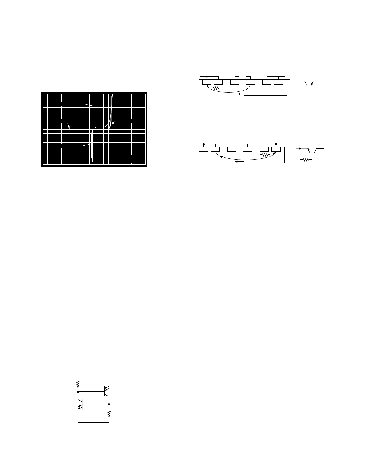
A quick analysis can be performed on site to evaluate if a
device may have been overstressed or may have been
subjected to an ESD event.
In order to perform this
analysis, to compare the pin-to-pin I/V results of the sus-
pect device to those of a known good device, a curve
tracer or similar equipment should be used. A typical
set of I/V traces for a short circuit, open circuit or ESD
leakage on a digital input pin (with reference to the V
SS
supply pin) of a 12-bit DAC is shown in Figure 7.
OPEN CIRCUIT
SHORT CIRCUIT
V/DIV. : 2V
I / DIV. : 50µA
GOOD TRACE
ESD LEAKAGE
Figure 7. Example of an Unpowered Curve Trace
Analysis of a Digital Pin versus a Supply Pin (V
SS
)
LATCH-UP
Latch-up is a potentially destructive situation in which a
parasitic active device is triggered, shorting the positive
and negative supplies together.
If current flow is not
limited, electrical overstress will occur.
The classic case
of latch-up occurs in CMOS output devices, in which the
driver transistors and wells form a
pnpn SCR structure
when one of the two parasitic base-emitter junctions is
momentarily forward biased during an overvoltage
event. The SCR turns on and essentially causes a short
between V
DD
and ground.
Triggering Mechanisms
There are two main triggering mechanisms.
First, if the
input/output (I/O) pin voltage is raised above the posi-
tive supply, or lowered below the negative supply, one
of the parasitic transistors is turned on. The current re-
turning to the supply through the collector causes a volt-
age drop across the base-emitter of the second parasitic
transistor. In turn, the collector current of the second
transistor maintains a forward bias on the base-emitter
of the first transistor. If the product of the two transistor
gains is greater than unity, the condition may be self-
sustaining and can persist even after the external volt-
age is removed.
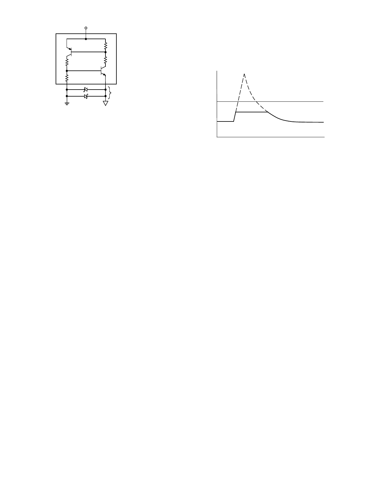
OUTPUT
V
DD
R
SUB
GND
RWELL
OUTPUT
QP
QN
Figure 8. Parasitic SCR. The Diffusions in a CMOS
output form a parasitic SCR. The resistors are labeled
for an n-well process.
This triggering mechanism can occur if excessive volt-
age overshoot is present at the I/O pin, or if the signal
arrives at the input before the power supplies are ap-
plied to the device, or due to electrostatic discharge.
This latch-up is usually limited to the devices directly
connected to the pin.
p+
n+
n+
p+
p+
n+
n-well
p-sub
GND
OUTPUT
OUTPUT
GND
V
DD
ε
–
+
V
DD
Figure 9a. Output Overvoltage Triggering. Initial hole
current flows when the output voltage is raised above
V
DD
. This current causes a voltage rise in the substrate
under the NMOS device.
p+
n+
n+
p+
p+
n+
n-well
p-sub
GND
OUTPUT
V
DD
OUTPUT
GND
R
SUB
ε
–
+
Figure 9b. Current Multiplication. The substrate
voltage rise actively biases the second parasitic
transistor into conduction. The electron current
subsequently causes a voltage drop in the n-well,
further turning on the first transistor. If the product of
the current gains is larger than one, the final current
flow between the supplies can be self-sustaining,
limited only by internal resistance’s, i.e., an SCR.
Although triggering is by an overvoltage event (typically
of only a diode drop above or below the power sup-
plies), the industry practice is to classify the I/O suscepti-
bility in terms of the amount of excess current the pin
can source or sink in this overvoltage condition before
the internal parasitic resistance's develop enough volt-
age drop to sustain the latch-up condition. A value of
100 mA is generally considered adequate, with 200 mA
considered immune to latch-up.
The
second triggering mechanism occurs if a supply
voltage is raised enough to break down an internal junc-
tion, injecting current into the SCR previously described.
This triggering mechanism can occur due to supply tran-
sients, or electrostatic discharges shunted to a supply
rail. Unlike the case of I/O triggering, latch-up can occur
anywhere on the die and is not limited to the vicinity of
the external power connections or I/O pins.
The susceptibility to power supply overvoltage is usu-
ally limited by the fabrication process on which the de-
vice is manufactured, and can be found in the data sheet
under the Absolute Maximum Rating specification.
If
this rating is exceeded, permanent EOS damage may
occur. Operating a device near the maximum ratings
may degrade the long term reliability of the device. Also
the electrical specifications are applicable only at the
supply specified on the data sheet and will not be guar-
anteed above these ratings.
–5–
Design Rules
The following is a set of rules to be followed for all de-
signers using CMOS and Bipolar-CMOS ICs:
5
1. Digital inputs and outputs should not be allowed to
exceed V
DD
by more than 0.3 volts at any time. This
includes a power-down situation when V
DD
= 0 volts.
2. Digital inputs and outputs should also not be allowed
to go below DGND by more than –0.3 volts.
3. For mixed signal devices, DGND should not be al-
lowed to exceed AGND by 0.3 volts.
4. For a CMOS or Bipolar-CMOS DAC, I
OUT
should, in
general, not be allowed to drop below AGND by more
than 0.3 volts. Some DACs can tolerate significant
I
OUT
current flow, however, without any danger of
latch-up.
Latch-Up Prevention Techniques
The following recommendations should be imple-
mented in general, for all applications with CMOS and
Bipolar-CMOS ICs that violate one or more of the previ-
ously discussed rules:
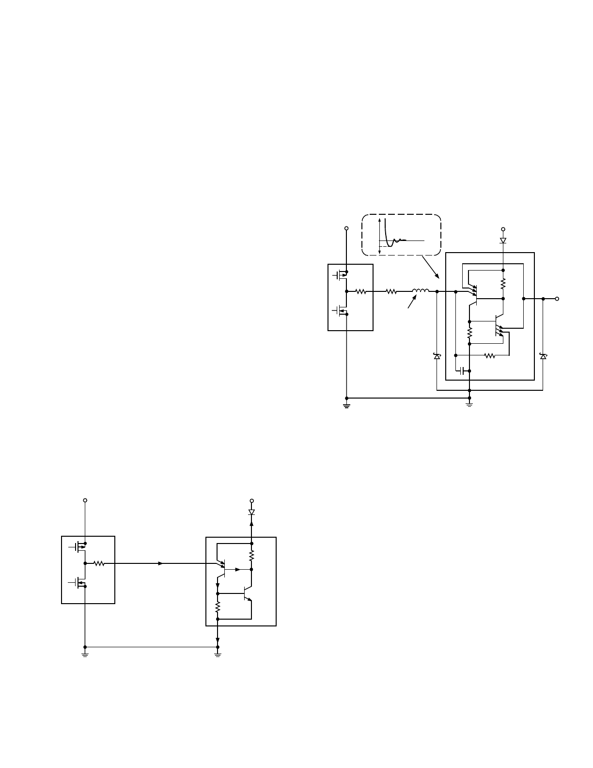
1. If the digital inputs or outputs of a device can go be-
yond V
DD
at any time, a diode (such as a 1N914) con-
nected in series with V
DD
will prevent SCR action and
subsequent latch-up. This works because the diode
prevents the base current of the parasitic lateral-PNP
transistor from flowing out the V
DD
pin, thus prevent-
ing SCR triggering. This is shown in Figure 10.
Diodes are also a reliable solution if power-up se-
quencing is identified as the failure mechanism. In
such a case, the insertion of a Schottky diode be-
tween the logic inputs and the V
DD
supply rail (the
anode of the diode connected to the logic inputs), will
ensure that the logic inputs do not exceed the V
DD
supply by more than 0.3 volts, thus preventing latch-
up of the device.
Ib
≈
0
Ic
=
0
R
p-well
I
DGND
≈
0
DGND
R
SUB
V
DD
IC POWERED UP
IC#1
R
OUT
IC#2
I
DD
≈
0
1N914
0V
+5V
IC POWERED DOWN
DGND
COMMON GROUND
OUTPUT
INPUT
I
IN
≈
0
V
DD
Figure 10. Adding an inexpensive silicon diode in
series with the V
DD
pin of the unpowered IC effec-
tively prevents the parasitic lateral-PNP transistor’s
base current from flowing and inhibits SCR action.
However, the one
exception to this rule is when the
input range of a device exceeds the supply voltage
range of the device, e.g., by design the AD7893-10 12-
bit A/D subsystem, the input range is
±
10 V and the
supply is +5 V.
2. If the digital inputs and outputs of a device can go
below DGND at any time, a Schottky diode (such as
an HP5082-2835) connected from those inputs or out-
puts to DGND will effectively clamp negative excur-
sions at –0.3 volts to –0.4 volts. This prevents the
emitter-base junction of the parasitic NPN transistor
from being turned on, and also prevents SCR
triggering. Figure 11 shows the connections for the
Schottky diodes.
R
p-well
DGND
R
SUB
V
DD
IC#1
R
OUT
IC#2
1N914
+5V
DGND
COMMON GROUND
V
DD
R
IN
C
IN
HP5082-
2835
L
R
DAMPING
PARASITIC
TRACE
INDUCTANCE
I/P
HP5082-
2835
OUTPUT
+5V
0V
–0.3
INPUT CLAMPED
AND DAMPED
Figure 11. Adding Schottky diodes from the inputs
and outputs of a CMOS IC to DGND protects against
undervoltages causing conduction of the parasitic
NPN, thus inhibiting SCR action. The series damp-
ing resistor makes ringing due to long PC board
traces die out more quickly.
3. If the DGND potential can occasionally exceed AGND
by more than 0.3 volts, a Schottky diode placed be-
tween the two pins of the device will prevent conduc-
tion of the associated parasitic NPN transistor. This
provides additional protection against latch-up as
shown in Figure 12. An extra diode connected in in-
verse parallel with the one just mentioned provides
clamping of DGND to AGND in the other direction
and will help to minimize digital noise from being in-
jected into the IC.
To identify over- and under-voltage events as described
in points (2) and (3) above, the use of a storage oscillo-
scope is suggested, set at the maximum ratings specifi-
cation for each pin. Set the Time/Div. to the minimum
setting on the oscilloscope (preferably in the ns range).
This test should be conducted over a long period of
time, e.g., overnight.
4. In circuits where the I
OUT
pin of a CMOS IC can be
pulled below AGND, another Schottky diode clamp
between these two terminals will prevent sensitive
–6–
LATERAL
PNP
VERTICAL
NPN
R3
R1
R2
R4
+5V
HP5082-2835
SCHOTTKY
DIODES
DGND
AGND
Figure 12. Connecting Schottky diodes between
DGND and AGND prevents conduction of the
parasitic NPN transistor, and helps to minimize
injected noise from DGND to the analog output.
ICs from latching up. This condition sometimes oc-
curs with high speed bipolar operational amplifiers
that are used as current-to-voltage converters follow-
ing a DAC. During power-up or power-down transi-
tions, the op amp’s inverting input presents a low
impedance from I
OUT
to the negative supply rail. An
unprotected DAC may fail without the recommended
Schottky diode clamp to AGND.
5. In designs that have long digital PC board traces be-
tween components and are therefore prone to induc-
tive ringing problems, a series damping resistor of
10
Ω
–100
Ω
will be beneficial. This resistor increases
the damping factor of the equivalent series RLC net-
work and causes the ringing to decay more quickly.
This will help to prevent conduction of the input or
output protection diodes.
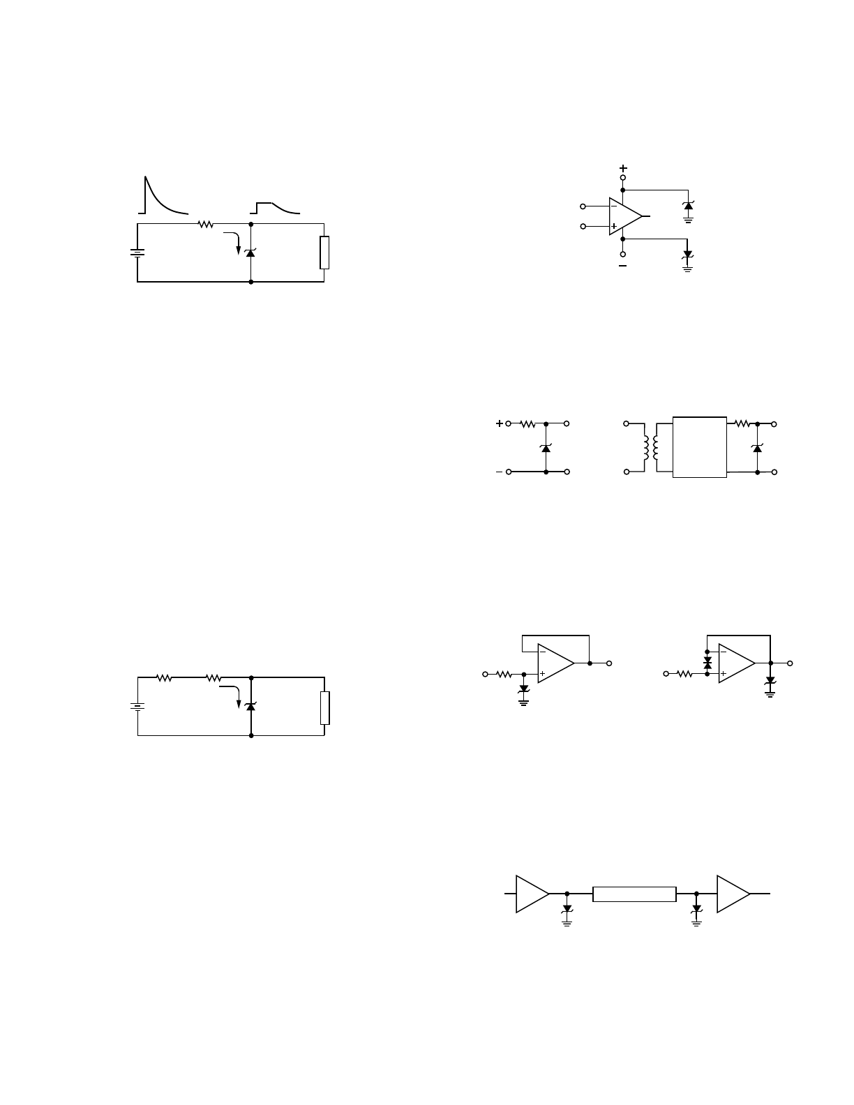
High Voltage Transients
If power supply overvoltaging is identified as the failure
mechanism, a reliable solution is the insertion of a
TransZorb* transient voltage suppressor (TVS). What is
a TVS and how does it work?
Transient voltage suppressors
6
(TVSs) are devices used
to protect vulnerable circuits from electrical overstress
such as that caused by ESD, inductive load switching
and lightning-induced line transients. Within the TVS,
damaging voltage spikes are limited by clamping or ava-
lanche action of a rugged silicon pn junction which re-
duces the amplitude of the transient to a nondestructive
level.
In a circuit, the TVS should be “invisible” until a
transient appears. Electrical parameters such as break-
down voltage (V
BR
), standby (leakage) current (I
D
), and
capacitance should have no effect on normal circuit
performance.
To limit standby current and to allow for variations in
V
BR
caused by the temperature coefficient of the TVS,
the TVS breakdown voltage is usually 10% above the
*TransZorb is a registered trademark of General Semiconductor
Industries, Inc.
reverse standoff voltage (V
R
), which approximates the
circuit absolute maximum operating voltage. When a
transient occurs, the TVS clamps instantly to limit the
spike voltage to a safe level, called the clamping voltage
(V
C
), while conducting potentially damaging current
away from the protected component.
TRANSIENT PEAK
IC FAILURE THRESHOLD
TVS CLAMPING
VOLTAGE (V
C
)
+30V
+20V
+12V
NORMAL OPERATING
VOLTAGE
TIME
Figure 13. Transients of several thousand volts can be
clamped to a safe level by the TVS.
TVSs are designed, specified and tested for transient
voltage protection, while a Zener diode is designed and
specified for voltage regulation.
Therefore, for transient
protection the TVS should be selected over the Zener.
The surge power and surge current capability of the
TVS are proportional to its junction area. Surge ratings
for silicon TVS families are normally specified in kilo-
watts of peak pulse power (P
P
) during a given waveform.
Early devices were specified with a 10/1000
µ
s wave-
form (10
µ
s rise to peak and 1000
µ
s exponential decay
to one half peak), while more recent devices are rated
for an 8/20
µ
s test waveform. Power ratings range from
5 kW for 10/1000
µ
s, down to 400 W for 8/20
µ
s. This
power is derived from the product of the peak voltage
across the TVS and the peak current conducted through
the device.
TVSs have circuit operating voltages available in incre-
ments from 5 V up to 376 V for some families. Because
of the broad range of voltages and power ratings avail-
able (as well as the universal presence of transient volt-
ages), TVSs are used in a wide variety of circuits and
applications.
As an example, consider a pressure transducer which
operates at 28 V, placed in an environment in which it
encounters a transient voltage of 140 V peak, having a
source impedance of 2
Ω
and a duration of 10/1000
µ
s.
The failure threshold of the transducer is 40 V, therefore
the TVS must clamp at 40 V or less.
The current deliv-
ered by this transient is:
I = (140 V – 40 V)/2
Ω
= 50 A
Note that the voltage clamping action of the TVS results
in a voltage divider whereby the open circuit voltage of
the transient appears across the combination of the
source impedance and the TVS device.
Thus the TVS
–7–
TYPICAL TVS APPLICATIONS
DC Line Applications
TransZorb TVSs on power lines prevent IC failures
caused by transients, power supply reversals or during
switching of the power supply between on and off
(Figure 16).
Ic
Figure 16.
For power sources utilizing the TransZorb TVS, the
TransZorb TVS is chosen such that the reverse stand-off
voltage is equal to or greater than the dc output voltage.
For certain applications it may be more desirable to re-
place the series resistor (R) with an inductor (Figure 17).
RECTIFIER
NETWORK
R
TO
LOAD
AC
INPUT
TO
LOAD
15V
DC
INPUT
R
Figure 17.
Signal Line Applications
Input pins are vulnerable to low energy, high voltage
static discharges or crosstalk transmitted to the signal
wires. Limited protection is provided by the clamp
diode or an input network within the IC substrate
(Figure 18).
Ic
Ic
OR
Figure 18.
Transients generated on the line can vary from a few mi-
croseconds to several milliseconds in duration and up to
10,000 volts in magnitude.
Excess current passing
through the diode can cause an open circuit condition or
a slow degradation of the circuit performance.
TransZorb TVSs located on the signal line can absorb
this excess energy (Figure 19).
SIGNAL WIRE
OUT
IN
Figure 19.
A further reference on the subject of using TransZorbs
for circuit protection is Analog Devices Application Note
AN-311, entitled ”How to Reliably Protect CMOS Circuits
against Power Supply Overvoltaging.“
clamping voltage is subtracted from the transient volt-
age leaving a net source voltage of 100
V. When the
clamping voltage is high compared to the transient peak
voltage, the current is significantly reduced.
This circuit can be protected with a 5 kW rated TransZorb
TVS which will easily sustain the surge current.
TRANSIENT
VOLTAGE
CLAMPED
TRANSIENT
28V
2
Ω
5kW
TVS
LOAD
Z
S
Figure 14. A 5 kW TVS is required to handle the surge
current.
An alternate and more economical approach is to add a
series resistor to effectively increase the source imped-
ance thus limiting surge current as illustrated in Figure
15. Since the current drawn by the transducer under
normal operation is small (<20 mA typical), perfor-
mance is not adversely affected by a reduction in supply
current.
For a small load current, 10 mA, the voltage drop across
the added resistance is minimal, about 250
mV for a
25 ohm resistor. Adding this resistor reduces the surge
current to:
I = (140 V – 40 V)/(2
Ω
+ 25
Ω
) = 3.7 A
This is less than one-tenth the surge current without the
resistor. A TVS with lower power rating is able to
handle the resulting current.
In this case a 500 W sup-
pressor replaces the 5 kW device, saving board space
and cost.
28V
2
Ω
500W
TVS
LOAD
25
Ω
Z
S
Figure 15. The series resistor reduces transient current
allowing a much smaller TVS to be used.
Carbon composition resistors are recommended for this
application because of their energy dissipation capabil-
ity. Steady state power dissipated by the resistor (V
×
I) is
2.5 mW requiring the lowest rated resistor available for
adequate margin.

–8–
E2054–15–8/95
PRINTED IN U.S.A.
IN SUMMARY
Designing an application with maximum protection of
the integrated circuits is a challenging problem with a
solution that depends on many factors. The following is
a brief summary of the protection schemes discussed in
this application note:
1. Personnel should be trained in the proper handling
techniques for prevention of EOS/ESD damage.
2. A good facilities ground system including shielding
of equipment and data lines should be implemented.
3. Use transient suppressors judiciously, i.e., check if
there are spikes on the supply and the ground lines
which may exceed the maximum ratings of those
pins.
4. Review the proper power-up sequence of the
device(s). The correct order should normally be:
GND, Main supplies (if possible the substrate supply
being first), V
CC
, V
REF+/–
and finally all other pins.
5. Review the data sheet, in particular the maximum rat-
ings section.
Remaining devices from a lot that may have been
mistested or subjected to the same conditions as those
of any failing devices should be evaluated to determine
if latent damage may be present.
This analysis should
be performed due to the possibility that overstress con-
ditions existed which did not cause immediate failure
but induced subtle damage that could result in long-
term reliability problems.
Finally, the issue of input overvoltage protection for am-
plifiers is not discussed in this application note. How-
ever, it is exclusively discussed in two other Analog
Devices publications; (1) Joe Buxton, ”Simple Tech-
niques Protect Amplifiers from Input Overvoltage,“
Ana-
log Dialogue 28-3, 1994, and (2) Joe Buxton, ”Input
Overvoltage Protection,“
System Applications Guide,
Analog Devices, 1993, pp 1–56 to 1–74.
REFERENCES
1
Henry Domingos, ”Circuit Design for EOS/ESD Protec-
tion,” Proc. 1982 EOS/ESD Symp., pp. 1–17 to 1–21.
2
John A. Schmidt, Manager of Technical Services IMCS
Corporation, Santa Clara, CA, ”CDM–The Newest ESD
Test Model,“ 1991.
3
MIL-STD-883 Method 3015, ”Electrostatic Discharge
Sensitivity Classification,“ Military Standard Test
Methods and Procedures for Microelectronics.
4
ESD Prevention Manual, 1986. Norwood MA; Analog
Devices Inc., pp 9-11. Contains additional references.
5
Mark Alexander, ”Understanding and Preventing
Latch-Up in CMOS DACs,“ AN-109. Free from Analog
Devices, PMI Division.
6
General Instrument, Power Semiconductor Division
Data Book/11th edition, pp. 633, 696–703. Contains ad-
ditional references.
Andrew Olney, Analog Devices, Inc., personal communication